

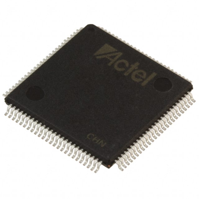
A54SX32A-TQG100
Product Overview
Category
The A54SX32A-TQG100 belongs to the category of programmable logic devices (PLDs).
Use
This product is primarily used in digital circuit design and implementation. It provides a flexible and customizable solution for various applications.
Characteristics
- Programmable: The A54SX32A-TQG100 can be programmed to perform specific functions based on user requirements.
- High Integration: It offers a high level of integration, allowing for complex designs to be implemented on a single chip.
- Versatile: This PLD supports a wide range of applications due to its programmability.
- Low Power Consumption: The A54SX32A-TQG100 is designed to operate efficiently with low power consumption.
Package
The A54SX32A-TQG100 comes in a TQG100 package.
Essence
The essence of this product lies in its ability to provide a reconfigurable hardware platform that can be tailored to meet specific design needs.
Packaging/Quantity
The A54SX32A-TQG100 is typically packaged individually and is available in various quantities depending on customer requirements.
Specifications
- Logic Elements: 54,000
- Flip-Flops: 32,000
- Maximum Frequency: 250 MHz
- I/O Pins: 100
- Operating Voltage: 3.3V
- Package Type: TQG100
Detailed Pin Configuration
The A54SX32A-TQG100 has a total of 100 pins, each serving a specific purpose. The pin configuration is as follows:
(Pin Number) - (Pin Name) - (Function)
1 - VCCIO - Power Supply for I/O Banks 2 - GND - Ground 3 - VCCINT - Internal Core Voltage 4 - GND - Ground 5 - IOB0 - I/O Bank 0 6 - IOB1 - I/O Bank 1 7 - IOB2 - I/O Bank 2 8 - IOB3 - I/O Bank 3 9 - ... (and so on)
Functional Features
- Reconfigurability: The A54SX32A-TQG100 can be reprogrammed multiple times, allowing for design modifications and updates.
- High-Speed Performance: With a maximum frequency of 250 MHz, this PLD offers fast and efficient operation.
- I/O Flexibility: The device provides a sufficient number of I/O pins to accommodate various input and output requirements.
- Design Security: The A54SX32A-TQG100 incorporates security features to protect intellectual property and prevent unauthorized access.
Advantages and Disadvantages
Advantages
- Flexibility: The programmable nature of the A54SX32A-TQG100 allows for customization and adaptability in different applications.
- Integration: Its high integration capability reduces the need for additional components, saving space and cost.
- Time-to-Market: Using this PLD can significantly reduce development time compared to designing custom circuits from scratch.
Disadvantages
- Learning Curve: Utilizing the full potential of the A54SX32A-TQG100 may require a learning curve for designers unfamiliar with programmable logic devices.
- Limited Resources: The available logic elements and I/O pins may not be sufficient for extremely complex designs.
Working Principles
The A54SX32A-TQG100 operates based on the principles of field-programmable gate arrays (FPGAs). It consists of configurable logic blocks (CLBs), interconnect resources, and I/O blocks. The CLBs contain look-up tables (LUTs) that can be programmed to implement desired logic functions. The interconnect resources allow for the routing of signals between different CLBs and I/O blocks. By configuring the LUTs and interconnects, designers can create custom digital circuits.
Detailed Application Field Plans
The A54SX32A-TQG100 finds applications in various fields, including:
- Communications: It can be used in networking equipment, routers, and communication protocols.
- Industrial Automation: This PLD is suitable for implementing control systems, motor drives, and sensor interfaces.
- Consumer Electronics: It can be utilized in smart home devices, gaming consoles, and multimedia systems.
- Automotive: The A54SX32A-TQG100 can be employed in automotive electronics, such as engine control units and infotainment systems.
- Medical Devices: It finds application in medical imaging, patient monitoring, and diagnostic equipment.
Detailed and Complete Alternative Models
- A54SX16A-TQG100
- A54SX72A-TQG100
- A54SX08A-TQG100
- A54SX32A-PQ208
- A54SX16A-PQ208
10个与A54SX32A-TQG100在技术解决方案中的应用相关的常见问题及解答
Sure! Here are 10 common questions and answers related to the application of A54SX32A-TQG100 in technical solutions:
Q: What is the A54SX32A-TQG100? A: The A54SX32A-TQG100 is a specific model of field-programmable gate array (FPGA) manufactured by Microsemi Corporation.
Q: What are the key features of the A54SX32A-TQG100? A: The A54SX32A-TQG100 offers 54,000 system gates, 32,768 macrocells, and operates at a maximum frequency of 100 MHz.
Q: How can the A54SX32A-TQG100 be used in technical solutions? A: The A54SX32A-TQG100 can be used for various applications such as digital signal processing, embedded systems, telecommunications, and industrial control systems.
Q: What programming languages are supported by the A54SX32A-TQG100? A: The A54SX32A-TQG100 can be programmed using Hardware Description Languages (HDLs) like VHDL or Verilog.
Q: Can the A54SX32A-TQG100 be reprogrammed after deployment? A: Yes, the A54SX32A-TQG100 is a reprogrammable FPGA, allowing for flexibility and updates to the design even after deployment.
Q: What tools are available for designing with the A54SX32A-TQG100? A: Microsemi provides Libero SoC Design Suite, which includes software tools for designing, simulating, and programming the A54SX32A-TQG100.
Q: What are the power requirements for the A54SX32A-TQG100? A: The A54SX32A-TQG100 typically operates at a voltage range of 3.3V, but it is recommended to refer to the datasheet for specific power requirements.
Q: Can the A54SX32A-TQG100 interface with other components or devices? A: Yes, the A54SX32A-TQG100 supports various communication interfaces such as SPI, I2C, UART, and GPIOs, allowing it to interface with other components or devices.
Q: Are there any limitations or considerations when using the A54SX32A-TQG100? A: Some considerations include the available resources (gates, macrocells), timing constraints, and power consumption, which should be carefully managed during design.
Q: Where can I find more information about the A54SX32A-TQG100? A: You can find detailed information, including datasheets, application notes, and reference designs, on Microsemi's official website or by contacting their technical support team.
Please note that the answers provided here are general and may vary depending on specific requirements and use cases.