

A54SX72A-2FGG256I
Product Overview
Category
The A54SX72A-2FGG256I belongs to the category of Field Programmable Gate Arrays (FPGAs).
Use
FPGAs are integrated circuits that can be programmed and reprogrammed to perform various digital functions. The A54SX72A-2FGG256I is specifically designed for applications requiring high-performance and flexibility.
Characteristics
- High-performance FPGA with advanced features
- Flexible and reprogrammable design
- Suitable for complex digital systems
- Offers a wide range of logic elements and I/O options
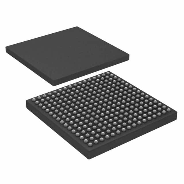
Package
The A54SX72A-2FGG256I comes in a compact and durable package, ensuring easy handling and protection during transportation and installation.
Essence
The essence of the A54SX72A-2FGG256I lies in its ability to provide a customizable and versatile solution for digital system design and implementation.
Packaging/Quantity
The A54SX72A-2FGG256I is typically packaged individually and is available in varying quantities depending on the customer's requirements.
Specifications
- FPGA Family: A54SX
- Logic Cells: 72,000
- Speed Grade: -2
- Package Type: FG256
- I/O Pins: 256
- Operating Voltage: 3.3V
- Maximum Frequency: 250 MHz
- Configuration Memory: 256 Kbits
Detailed Pin Configuration
The A54SX72A-2FGG256I has 256 I/O pins, each serving a specific purpose in the overall functionality of the FPGA. For detailed pin configuration information, please refer to the product datasheet or user manual provided by the manufacturer.
Functional Features
- High-speed performance
- Reconfigurable architecture
- Support for various communication protocols
- Embedded memory blocks for efficient data storage
- Flexible I/O options for interfacing with external devices
Advantages and Disadvantages
Advantages
- High level of customization and flexibility
- Faster time-to-market compared to custom ASIC designs
- Lower development costs compared to ASICs
- Ability to reprogram the FPGA for different applications
Disadvantages
- Higher power consumption compared to dedicated hardware solutions
- Limited performance compared to specialized ASICs in certain applications
- Steeper learning curve for programming and utilizing FPGAs effectively
Working Principles
The A54SX72A-2FGG256I operates based on the principles of digital logic design. It consists of a large number of configurable logic blocks interconnected through programmable routing resources. These logic blocks can be programmed to implement various digital functions, allowing the FPGA to perform complex tasks.
Detailed Application Field Plans
The A54SX72A-2FGG256I finds applications in a wide range of fields, including but not limited to: - Telecommunications - Industrial automation - Aerospace and defense - Medical equipment - Automotive electronics
Detailed and Complete Alternative Models
- A54SX16A-2FGG256I: Smaller version with 16,000 logic cells and 256 I/O pins.
- A54SX144A-2FGG256I: Larger version with 144,000 logic cells and 256 I/O pins.
- A54SX36A-2FGG256I: Intermediate version with 36,000 logic cells and 256 I/O pins.
These alternative models offer varying levels of logic capacity while maintaining the same pin configuration and package type as the A54SX72A-2FGG256I.
In conclusion, the A54SX72A-2FGG256I is a high-performance FPGA that provides flexibility and customization for various digital system applications. Its advanced features, wide range of I/O options, and reprogrammable design make it a versatile choice for designers in multiple industries.
10个与A54SX72A-2FGG256I在技术解决方案中的应用相关的常见问题及解答
Sure! Here are 10 common questions and answers related to the application of A54SX72A-2FGG256I in technical solutions:
Q: What is the A54SX72A-2FGG256I? A: The A54SX72A-2FGG256I is a specific model of field-programmable gate array (FPGA) manufactured by Microsemi.
Q: What are the key features of the A54SX72A-2FGG256I? A: The A54SX72A-2FGG256I offers 54,000 logic cells, 72 macrocells, and comes in a 256-pin FineLine BGA package.
Q: What are the typical applications for the A54SX72A-2FGG256I? A: The A54SX72A-2FGG256I is commonly used in various technical solutions such as telecommunications, industrial automation, aerospace, and defense.
Q: Can the A54SX72A-2FGG256I be reprogrammed? A: Yes, the A54SX72A-2FGG256I is a field-programmable device, meaning it can be reprogrammed multiple times to suit different applications.
Q: What programming languages can be used with the A54SX72A-2FGG256I? A: The A54SX72A-2FGG256I can be programmed using hardware description languages (HDLs) like VHDL or Verilog.
Q: How does the A54SX72A-2FGG256I interface with other components in a system? A: The A54SX72A-2FGG256I can interface with other components through various standard protocols such as SPI, I2C, UART, and GPIO.
Q: What are the power requirements for the A54SX72A-2FGG256I? A: The A54SX72A-2FGG256I typically operates at a voltage range of 1.8V to 3.3V, depending on the specific design requirements.
Q: Can the A54SX72A-2FGG256I handle high-speed data processing? A: Yes, the A54SX72A-2FGG256I is capable of handling high-speed data processing due to its advanced architecture and optimized circuitry.
Q: Are there any development tools available for programming the A54SX72A-2FGG256I? A: Yes, Microsemi provides development tools like Libero SoC Design Suite and SoftConsole IDE that support programming and debugging of the A54SX72A-2FGG256I.
Q: Where can I find additional technical documentation and support for the A54SX72A-2FGG256I? A: You can find detailed technical documentation, datasheets, application notes, and support resources on Microsemi's official website or by contacting their customer support team.
Please note that the answers provided here are general and may vary based on specific implementation requirements and manufacturer guidelines.