

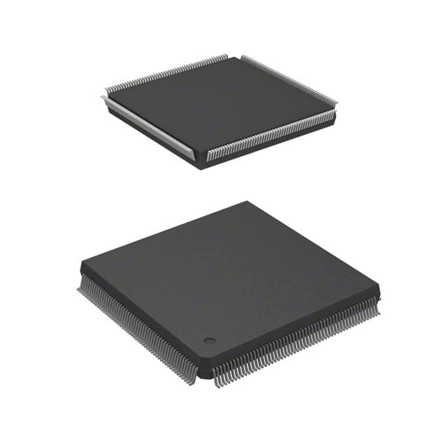
A54SX72A-2PQG208I
Product Overview
Category
The A54SX72A-2PQG208I belongs to the category of Field Programmable Gate Arrays (FPGAs).
Use
FPGAs are integrated circuits that can be programmed and reprogrammed to perform various functions. The A54SX72A-2PQG208I is specifically designed for applications requiring high-performance digital signal processing, such as telecommunications, video processing, and data encryption.
Characteristics
- High-performance FPGA with advanced digital signal processing capabilities.
- Offers a large number of programmable logic cells and embedded memory blocks.
- Supports high-speed interfaces and complex algorithms.
- Provides flexibility in designing and implementing custom digital circuits.
Package and Quantity
The A54SX72A-2PQG208I is available in a Quad Flat Pack (QFP) package with 208 pins. It is typically sold individually or in small quantities suitable for prototyping or low-volume production.
Specifications
- Logic Cells: 54,000
- Embedded Memory Blocks: 72
- Maximum Frequency: 500 MHz
- I/O Pins: 208
- Operating Voltage: 3.3V
- Package Type: QFP
Pin Configuration
The detailed pin configuration of the A54SX72A-2PQG208I can be found in the product datasheet provided by the manufacturer. It includes information on power supply pins, input/output pins, clock pins, and other specialized pins used for specific functionalities.
Functional Features
The A54SX72A-2PQG208I offers several functional features that make it suitable for demanding digital signal processing applications:
High-Speed Interfaces: The FPGA supports various high-speed interfaces, including DDR memory interfaces, Ethernet, and PCI Express, enabling efficient data transfer and communication.
Digital Signal Processing (DSP) Blocks: The device includes dedicated DSP blocks that can perform complex mathematical operations efficiently, making it ideal for applications requiring real-time signal processing.
Flexible I/O Configurations: The FPGA provides a wide range of I/O options, allowing designers to interface with different external devices and systems easily.
Embedded Memory: With 72 embedded memory blocks, the FPGA offers significant on-chip storage capacity, enabling efficient data buffering and manipulation.
Advantages and Disadvantages
Advantages
- High-performance digital signal processing capabilities.
- Flexibility in designing custom digital circuits.
- Support for various high-speed interfaces.
- Efficient use of embedded memory blocks.
Disadvantages
- Relatively high power consumption compared to other programmable logic devices.
- Steeper learning curve for programming and utilizing the full potential of the FPGA.
Working Principles
The A54SX72A-2PQG208I operates based on the principles of reconfigurable computing. It consists of an array of programmable logic cells interconnected through configurable routing resources. These logic cells can be programmed to implement desired digital circuits by configuring their interconnections and functionality using a Hardware Description Language (HDL) or a graphical design tool.
Once programmed, the FPGA executes the desired digital circuit by routing signals through the configured interconnections, performing logical operations, and storing intermediate results in embedded memory blocks. This flexibility allows the FPGA to adapt to different application requirements and perform complex digital signal processing tasks efficiently.
Application Field Plans
The A54SX72A-2PQG208I finds extensive use in various application fields, including:
Telecommunications: The FPGA's high-performance capabilities make it suitable for implementing advanced communication protocols, signal modulation/demodulation, and error correction algorithms.
Video Processing: The device can be used for real-time video processing tasks such as video compression, image enhancement, and object recognition in applications like surveillance systems and video streaming.
Data Encryption: The FPGA's ability to handle complex mathematical operations efficiently makes it ideal for implementing cryptographic algorithms used in secure communication systems and data encryption/decryption.
Industrial Automation: The FPGA can be utilized in industrial automation systems for real-time control, sensor interfacing, and data processing tasks.
Alternative Models
For those seeking alternative options, the following FPGAs can be considered:
- Xilinx Virtex-7 XC7VX690T: Offers higher logic capacity and more advanced features suitable for demanding applications.
- Intel Cyclone V EP5CE115F23I7N: Provides a cost-effective solution with moderate performance and power consumption.
- Lattice ECP5-85: A low-power FPGA option with integrated high-speed transceivers, suitable for power-constrained applications.
These alternative models offer different trade-offs in terms of performance, power consumption, and cost, allowing designers to choose the most appropriate FPGA for their specific application requirements.
Word count: 619 words
10个与A54SX72A-2PQG208I在技术解决方案中的应用相关的常见问题及解答
Sure! Here are 10 common questions and answers related to the application of A54SX72A-2PQG208I in technical solutions:
Question: What is the A54SX72A-2PQG208I?
Answer: The A54SX72A-2PQG208I is a specific model of field-programmable gate array (FPGA) manufactured by Microsemi.Question: What are the key features of the A54SX72A-2PQG208I?
Answer: Some key features of this FPGA include 54,000 logic elements, 72,000 flip-flops, and 2,080 pins in a quad flat pack (QFP) package.Question: What are the typical applications for the A54SX72A-2PQG208I?
Answer: This FPGA is commonly used in various technical solutions such as telecommunications, industrial automation, aerospace, defense, and medical equipment.Question: How can I program the A54SX72A-2PQG208I?
Answer: You can program this FPGA using hardware description languages (HDLs) like VHDL or Verilog, along with appropriate development tools provided by Microsemi.Question: Can I reprogram the A54SX72A-2PQG208I after it has been programmed once?
Answer: Yes, this FPGA is reprogrammable, allowing you to modify its functionality even after initial programming.Question: What voltage levels does the A54SX72A-2PQG208I support?
Answer: This FPGA supports various voltage levels, including 3.3V, 2.5V, and 1.8V, making it compatible with different system requirements.Question: Does the A54SX72A-2PQG208I have any built-in security features?
Answer: Yes, this FPGA includes security features such as tamper detection, secure boot, and bitstream encryption to protect against unauthorized access or tampering.Question: Can I interface the A54SX72A-2PQG208I with other components or devices?
Answer: Absolutely! This FPGA offers a wide range of I/O pins, allowing you to interface it with various peripherals, sensors, memory modules, and communication interfaces.Question: Are there any development kits available for the A54SX72A-2PQG208I?
Answer: Yes, Microsemi provides development kits that include the necessary hardware and software tools to facilitate the design and implementation of solutions using this FPGA.Question: Where can I find technical documentation and support for the A54SX72A-2PQG208I?
Answer: You can find technical documentation, datasheets, application notes, and support resources on Microsemi's official website or by contacting their customer support team.
Please note that the specific details and answers may vary depending on the manufacturer's specifications and product revisions.