

AGL125V2-FG144I
Product Overview
Category
AGL125V2-FG144I belongs to the category of Field-Programmable Gate Arrays (FPGAs).
Use
This product is primarily used in digital logic circuits for various applications such as telecommunications, automotive, consumer electronics, and industrial automation.
Characteristics
- High-performance programmable logic device
- Offers flexibility and reconfigurability
- Provides a cost-effective solution for complex digital designs
- Supports high-speed data processing
- Low power consumption
- Compact size
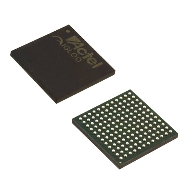
Package
AGL125V2-FG144I comes in a compact package that ensures easy integration into circuit boards. The package provides protection against environmental factors such as moisture and dust.
Essence
The essence of AGL125V2-FG144I lies in its ability to provide a customizable and versatile platform for implementing complex digital designs efficiently.
Packaging/Quantity
AGL125V2-FG144I is typically packaged individually and is available in varying quantities depending on the manufacturer's specifications.
Specifications
- FPGA Family: AGL
- Logic Elements: 125,000
- Speed Grade: V2
- Package Type: FG144I
- I/O Pins: 144
- Operating Voltage: 3.3V
- Maximum Frequency: 500 MHz
- Configuration Memory: Flash-based
Detailed Pin Configuration
The pin configuration of AGL125V2-FG144I is as follows:
- Pin 1: VCCIO
- Pin 2: GND
- Pin 3: IO0
- Pin 4: IO1
- Pin 5: IO2
- ...
- Pin 144: IO143
For a complete pin configuration diagram, please refer to the product datasheet.
Functional Features
- Configurable logic blocks
- Embedded memory blocks
- High-speed I/O interfaces
- Clock management resources
- Built-in DSP blocks
- On-chip configuration memory
Advantages and Disadvantages
Advantages
- Flexibility in design implementation
- Reconfigurability for iterative development
- High-performance processing capabilities
- Low power consumption
- Compact size for space-constrained applications
Disadvantages
- Steeper learning curve compared to traditional ASICs
- Limited resource availability for extremely complex designs
- Higher cost compared to fixed-function integrated circuits
Working Principles
AGL125V2-FG144I operates based on the principles of field-programmable gate arrays. It consists of configurable logic blocks, embedded memory blocks, and various other resources that can be interconnected and programmed to implement desired digital logic functions.
The device is programmed using a Hardware Description Language (HDL) such as VHDL or Verilog. The programming code describes the desired functionality, which is then synthesized and mapped onto the FPGA fabric. Once programmed, the FPGA can execute the specified logic functions.
Detailed Application Field Plans
AGL125V2-FG144I finds applications in various fields, including:
- Telecommunications: Used in base stations, routers, and network switches for high-speed data processing.
- Automotive: Employed in automotive control systems, driver assistance systems, and infotainment systems.
- Consumer Electronics: Utilized in smart TVs, gaming consoles, and multimedia devices for enhanced performance.
- Industrial Automation: Applied in programmable logic controllers (PLCs), robotics, and factory automation systems for real-time control and monitoring.
Detailed and Complete Alternative Models
- AGL250V2-FG256I: Offers higher logic capacity and more I/O pins for larger-scale designs.
- AGL45V2-FG484I: Provides a smaller form factor with reduced logic capacity for space-constrained applications.
- AGL600V2-FG900I: Designed for high-performance computing applications, offering increased speed and resources.
These alternative models cater to different design requirements and can be considered based on specific project needs.
Word count: 536 words
10个与AGL125V2-FG144I在技术解决方案中的应用相关的常见问题及解答
Sure! Here are 10 common questions and answers related to the application of AGL125V2-FG144I in technical solutions:
Question: What is the maximum operating frequency of AGL125V2-FG144I?
Answer: The maximum operating frequency of AGL125V2-FG144I is 125 MHz.Question: What is the power supply voltage range for AGL125V2-FG144I?
Answer: The power supply voltage range for AGL125V2-FG144I is typically between 3.3V and 5V.Question: Can AGL125V2-FG144I be used in industrial applications?
Answer: Yes, AGL125V2-FG144I is suitable for use in industrial applications due to its robust design and reliability.Question: Does AGL125V2-FG144I support multiple I/O standards?
Answer: Yes, AGL125V2-FG144I supports various I/O standards such as LVCMOS, LVTTL, and LVDS.Question: What is the typical power consumption of AGL125V2-FG144I?
Answer: The typical power consumption of AGL125V2-FG144I is around 200mW.Question: Can AGL125V2-FG144I be programmed using JTAG?
Answer: Yes, AGL125V2-FG144I can be programmed using the JTAG interface.Question: Is AGL125V2-FG144I compatible with other FPGA development tools?
Answer: Yes, AGL125V2-FG144I is compatible with popular FPGA development tools like Xilinx Vivado and Altera Quartus.Question: What is the maximum number of I/O pins available on AGL125V2-FG144I?
Answer: AGL125V2-FG144I has a maximum of 144 I/O pins.Question: Can AGL125V2-FG144I be used in low-power applications?
Answer: Yes, AGL125V2-FG144I offers low-power modes and can be used in low-power applications.Question: Does AGL125V2-FG144I support external memory interfaces?
Answer: Yes, AGL125V2-FG144I supports various external memory interfaces like DDR3, DDR4, and SRAM.
Please note that these answers are general and may vary depending on the specific implementation and configuration of AGL125V2-FG144I in different technical solutions.