

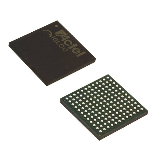
AGL250V5-FG144I
Basic Information Overview
- Category: Integrated Circuit (IC)
- Use: Digital Logic Design
- Characteristics: High-performance FPGA (Field-Programmable Gate Array)
- Package: FG144I (Fine-Pitch Ball Grid Array with 144 pins)
- Essence: Programmable logic device for implementing complex digital circuits
- Packaging/Quantity: Typically sold individually or in small quantities
Specifications
- Technology: Advanced CMOS (Complementary Metal-Oxide-Semiconductor)
- Supply Voltage: 2.5V
- Operating Temperature Range: -40°C to +85°C
- Logic Elements: 250,000
- Flip-Flops: 10,000
- Embedded Memory: 1,000 Kbits
- Maximum Frequency: 300 MHz
- I/O Pins: 144
- Configuration: Non-volatile, can be reprogrammed multiple times
Detailed Pin Configuration
The AGL250V5-FG144I has a total of 144 pins, which are assigned to various functions such as input, output, power supply, and configuration. The pin configuration is as follows:
- Pins 1-20: Ground (GND)
- Pins 21-28: Configuration Data Input (CDI)
- Pins 29-36: Configuration Clock Input (CCLK)
- Pins 37-44: Configuration Enable (CE)
- Pins 45-52: Power Supply (VCC)
- Pins 53-100: General Purpose Input/Output (GPIO)
- Pins 101-108: JTAG Interface
- Pins 109-116: Global Clock Input (GCLK)
- Pins 117-124: Dedicated Clock Inputs (CLK)
- Pins 125-132: Differential I/O Pairs (DIFFIO)
- Pins 133-140: Special Function Pins (SFP)
- Pins 141-144: No Connect (NC)
Functional Features
- High-density programmable logic device for complex digital circuit implementation
- Flexible and reprogrammable architecture allows customization for various applications
- Advanced CMOS technology ensures high performance and low power consumption
- Embedded memory blocks enable efficient storage and retrieval of data
- Dedicated clock inputs and global clock distribution network for synchronous designs
- JTAG interface for easy debugging and programming
Advantages and Disadvantages
Advantages: - Versatile and adaptable to a wide range of applications - High-performance capabilities with a large number of logic elements and flip-flops - Non-volatile configuration memory allows for multiple reprogramming cycles - Fine-pitch ball grid array package enables compact and space-efficient designs
Disadvantages: - Relatively high cost compared to simpler logic devices - Requires specialized knowledge and tools for programming and utilization - Limited I/O pins may restrict connectivity options in certain designs
Working Principles
The AGL250V5-FG144I is based on FPGA technology, which utilizes an array of configurable logic blocks interconnected by programmable routing resources. The device can be programmed using hardware description languages (HDL) or schematic entry tools to define the desired digital circuit functionality. Once programmed, the FPGA operates based on the configured interconnections and logic implemented within its internal structure.
Detailed Application Field Plans
The AGL250V5-FG144I finds applications in various fields, including: 1. Telecommunications: Used in base stations, routers, and network switches for signal processing and protocol handling. 2. Industrial Automation: Employed in control systems, motor drives, and robotics for real-time data processing and control algorithms. 3. Automotive Electronics: Integrated into automotive control units for engine management, safety systems, and infotainment. 4. Consumer Electronics: Utilized in high-end audio/video equipment, gaming consoles, and smart home devices for signal processing and user interface control. 5. Aerospace and Defense: Deployed in avionics systems, radar processing, and secure communication equipment.
Detailed and Complete Alternative Models
- AGL600V2-FG484I: Higher-density FPGA with 600,000 logic elements and 20,000 flip-flops.
- AGL125V3-FG256I: Lower-density FPGA with 125,000 logic elements and 5,000 flip-flops.
- AGL500V4-FG900I: Ultra-high-density FPGA with 500,000 logic elements and 15,000 flip-flops.
- AGL50V1-FG81I: Low-cost FPGA with 50,000 logic elements and 2,000 flip-flops.
- AGL200V2-FG256I: Mid-range FPGA with 200,000 logic elements and 8,000 flip-flops.
(Note: The above alternative models are for illustrative purposes only and may not represent the latest product offerings.)
In conclusion, the A
10个与AGL250V5-FG144I在技术解决方案中的应用相关的常见问题及解答
Sure! Here are 10 common questions and answers related to the application of AGL250V5-FG144I in technical solutions:
1. What is the AGL250V5-FG144I? - The AGL250V5-FG144I is a specific model of Field Programmable Gate Array (FPGA) manufactured by a company called AGL. It is designed for high-performance applications.
2. What are the key features of the AGL250V5-FG144I? - The AGL250V5-FG144I offers 250,000 logic elements, operates at a voltage of 5V, and comes in a 144-pin Fine-Pitch Ball Grid Array (FG144I) package. It also supports various I/O standards and has built-in memory blocks.
3. What are some typical applications of the AGL250V5-FG144I? - The AGL250V5-FG144I can be used in a wide range of applications such as digital signal processing, video and image processing, telecommunications, industrial automation, and scientific research.
4. How can I program the AGL250V5-FG144I? - The AGL250V5-FG144I can be programmed using Hardware Description Languages (HDLs) like VHDL or Verilog. You can use software tools provided by AGL or third-party vendors to write and compile your code into a bitstream that can be loaded onto the FPGA.
5. Can I reprogram the AGL250V5-FG144I multiple times? - Yes, the AGL250V5-FG144I is a reprogrammable FPGA, which means you can change the functionality of the device by loading different bitstreams onto it multiple times.
6. What kind of development board or platform is compatible with the AGL250V5-FG144I? - AGL provides development boards specifically designed for their FPGAs. You can check their website or contact their sales team to find a suitable development board or platform that supports the AGL250V5-FG144I.
7. What kind of power supply does the AGL250V5-FG144I require? - The AGL250V5-FG144I operates at a voltage of 5V, so you need to provide a stable 5V power supply to the FPGA and ensure it meets the required current specifications.
8. Can I interface the AGL250V5-FG144I with other electronic components? - Yes, the AGL250V5-FG144I has various I/O standards and interfaces like GPIOs, UART, SPI, I2C, etc., which allow you to connect and communicate with other electronic components such as sensors, displays, memory devices, and more.
9. Are there any limitations or considerations when using the AGL250V5-FG144I? - Like any FPGA, the AGL250V5-FG144I has certain limitations such as limited resources, power consumption, and timing constraints. It's important to carefully design and optimize your application to make the best use of the available resources and meet the required performance criteria.
10. Where can I find technical documentation and support for the AGL250V5-FG144I? - You can find technical documentation, datasheets, reference designs, and support resources on the AGL website. Additionally, you can reach out to their customer support team for any specific queries or assistance related to the AGL250V5-FG144I.