

AX1000-FG484I
Product Overview
Category
AX1000-FG484I belongs to the category of Field-Programmable Gate Arrays (FPGAs).
Use
This product is primarily used in digital logic circuits for various applications such as telecommunications, automotive, aerospace, and consumer electronics.
Characteristics
- High-performance programmable logic device
- Offers flexibility and reconfigurability
- Provides a wide range of logic gates, flip-flops, and memory blocks
- Can be customized to meet specific design requirements
Package
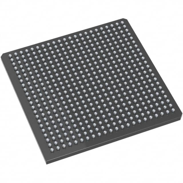
The AX1000-FG484I comes in a compact FG484 package, which ensures easy integration into electronic systems.
Essence
The essence of this product lies in its ability to provide a versatile platform for implementing complex digital designs with high performance and flexibility.
Packaging/Quantity
The AX1000-FG484I is typically packaged individually and is available in varying quantities depending on customer requirements.
Specifications
- Logic Elements: 1000
- Flip-Flops: 500
- Memory Blocks: 20
- Maximum Frequency: 500 MHz
- Operating Voltage: 1.2V
- I/O Pins: 200
- Package Type: FG484
Detailed Pin Configuration
The AX1000-FG484I has a total of 200 I/O pins, each serving a specific purpose in the overall functionality of the FPGA. The detailed pin configuration can be found in the product datasheet.
Functional Features
- High-speed data processing capabilities
- Configurable logic elements for custom designs
- On-chip memory blocks for efficient data storage
- Support for various communication protocols
- Built-in clock management resources
- Integrated power management features
Advantages and Disadvantages
Advantages
- Flexibility in design implementation
- Reconfigurability for iterative development
- High-performance computing capabilities
- Support for complex algorithms and processing tasks
Disadvantages
- Higher power consumption compared to fixed-function ASICs
- Longer development time due to design complexity
- Limited availability of specialized technical expertise
Working Principles
The AX1000-FG484I operates based on the principles of digital logic circuits. It consists of configurable logic elements, flip-flops, and memory blocks that can be programmed to perform specific functions. The FPGA is configured using a hardware description language (HDL) and can be reprogrammed multiple times to adapt to changing requirements.
Detailed Application Field Plans
The AX1000-FG484I finds applications in various fields, including:
- Telecommunications: Used in network routers, switches, and communication equipment for high-speed data processing.
- Automotive: Employed in automotive control systems, driver assistance systems, and infotainment systems.
- Aerospace: Utilized in satellite communication systems, onboard computers, and avionics.
- Consumer Electronics: Integrated into gaming consoles, multimedia devices, and smart home appliances.
Detailed and Complete Alternative Models
- AX500-FG256I: A lower-cost alternative with 500 logic elements and 256 I/O pins.
- AX2000-FG676I: A higher-performance alternative with 2000 logic elements and 676 I/O pins.
- AX5000-FG900I: A high-density alternative with 5000 logic elements and 900 I/O pins.
These alternative models offer varying levels of performance, I/O capabilities, and cost-effectiveness to cater to different project requirements.
Word count: 450 words
10个与AX1000-FG484I在技术解决方案中的应用相关的常见问题及解答
Sure! Here are 10 common questions and answers related to the application of AX1000-FG484I in technical solutions:
Q: What is AX1000-FG484I? A: AX1000-FG484I is a specific model of FPGA (Field-Programmable Gate Array) manufactured by a company called Xilinx.
Q: What are the key features of AX1000-FG484I? A: Some key features of AX1000-FG484I include a high-density programmable logic, embedded memory blocks, DSP slices, and various I/O options.
Q: What are the typical applications of AX1000-FG484I? A: AX1000-FG484I can be used in a wide range of applications such as telecommunications, automotive electronics, industrial automation, aerospace, and defense systems.
Q: How can AX1000-FG484I be programmed? A: AX1000-FG484I can be programmed using hardware description languages (HDLs) like VHDL or Verilog, which allow users to define the desired functionality of the FPGA.
Q: Can AX1000-FG484I be reprogrammed after deployment? A: Yes, AX1000-FG484I is a field-programmable device, meaning it can be reprogrammed even after it has been deployed in a system.
Q: What tools are available for programming AX1000-FG484I? A: Xilinx provides software tools like Vivado Design Suite that enable users to design, simulate, and program AX1000-FG484I.
Q: What is the power consumption of AX1000-FG484I? A: The power consumption of AX1000-FG484I depends on the specific design and usage scenario. It is important to refer to the datasheet or consult Xilinx for accurate power consumption information.
Q: Can AX1000-FG484I interface with other components or devices? A: Yes, AX1000-FG484I supports various I/O standards and can interface with other components or devices such as sensors, memory modules, communication interfaces, and more.
Q: Are there any limitations or considerations when using AX1000-FG484I? A: Some considerations include the need for proper cooling, managing power supply requirements, understanding timing constraints, and ensuring compatibility with other system components.
Q: Where can I find additional resources or support for AX1000-FG484I? A: Xilinx provides comprehensive documentation, application notes, forums, and technical support to assist users in utilizing AX1000-FG484I effectively.