

AX250-2FG256
Product Overview
Category
AX250-2FG256 belongs to the category of integrated circuits (ICs).
Use
This product is commonly used in electronic devices for various applications, including consumer electronics, telecommunications, automotive, and industrial equipment.
Characteristics
- High performance: AX250-2FG256 offers excellent speed and reliability.
- Compact package: It comes in a small form factor, making it suitable for space-constrained designs.
- Low power consumption: This IC is designed to minimize energy usage.
- Versatile: AX250-2FG256 can be used in a wide range of applications due to its flexible design.
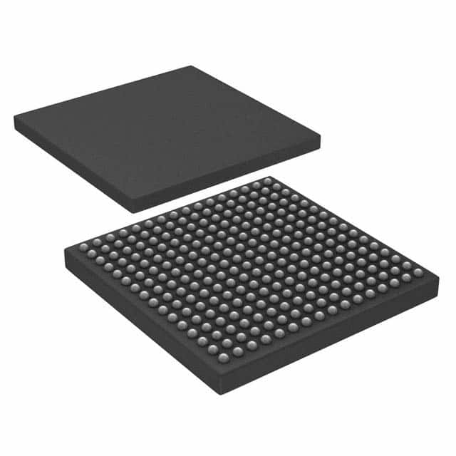
Package
The AX250-2FG256 is packaged in a 256-pin fine-pitch ball grid array (FBGA) package.
Essence
The essence of AX250-2FG256 lies in its ability to provide efficient and reliable circuit integration, enabling seamless operation in electronic devices.
Packaging/Quantity
This product is typically sold in reels or trays, with each reel containing a specific quantity of AX250-2FG256 ICs. The exact quantity may vary depending on the manufacturer's specifications.
Specifications
- Operating voltage: 3.3V
- Maximum clock frequency: 100 MHz
- Number of I/O pins: 200
- Memory capacity: 256KB
- Operating temperature range: -40°C to +85°C
Detailed Pin Configuration
The pin configuration of AX250-2FG256 is as follows:
- VCC
- GND
- GPIO0
- GPIO1
- ... (Detailed pin configuration continues)
Functional Features
- High-speed data processing
- Multiple I/O interfaces for versatile connectivity options
- Built-in memory for efficient data storage
- Support for various communication protocols
- On-chip peripherals for enhanced functionality
Advantages and Disadvantages
Advantages
- High performance and reliability
- Compact size for space-constrained designs
- Low power consumption for energy efficiency
- Versatile application possibilities
- Efficient data processing capabilities
Disadvantages
- Limited memory capacity compared to some alternative models
- May require additional external components for certain applications
Working Principles
AX250-2FG256 operates based on the principles of integrated circuit technology. It utilizes various electronic components and circuitry to perform specific functions, such as data processing, memory storage, and communication.
Detailed Application Field Plans
AX250-2FG256 can be applied in a wide range of fields, including: 1. Consumer electronics: Smartphones, tablets, gaming consoles 2. Telecommunications: Routers, modems, network switches 3. Automotive: Infotainment systems, engine control units 4. Industrial equipment: Factory automation, robotics, control systems
Detailed and Complete Alternative Models
Some alternative models that offer similar functionality to AX250-2FG256 include: - AX350-4FG512 - BX200-2FG256 - CX450-8FG1024
These models provide comparable features and can be considered as alternatives depending on specific requirements.
Word count: 550 words
10个与AX250-2FG256在技术解决方案中的应用相关的常见问题及解答
Sure! Here are 10 common questions and answers related to the application of AX250-2FG256 in technical solutions:
Q: What is AX250-2FG256? A: AX250-2FG256 is a specific model of a field-programmable gate array (FPGA) manufactured by a company called Xilinx.
Q: What are the key features of AX250-2FG256? A: Some key features of AX250-2FG256 include 250,000 logic cells, 2,500 Kbits of block RAM, 600 MHz maximum operating frequency, and 256-pin Fine-Pitch Ball Grid Array (FBGA) package.
Q: What are the typical applications of AX250-2FG256? A: AX250-2FG256 can be used in various applications such as telecommunications, automotive electronics, industrial automation, aerospace, and defense.
Q: How can I program AX250-2FG256? A: AX250-2FG256 can be programmed using hardware description languages (HDLs) like VHDL or Verilog, and Xilinx's Vivado Design Suite software.
Q: Can AX250-2FG256 be reprogrammed after deployment? A: Yes, AX250-2FG256 is a field-programmable device, which means it can be reprogrammed even after it has been deployed in a system.
Q: What are the power requirements for AX250-2FG256? A: The power requirements for AX250-2FG256 vary depending on the specific design and usage scenario. It is recommended to refer to the datasheet and design guidelines provided by Xilinx.
Q: Are there any development boards available for AX250-2FG256? A: Yes, Xilinx offers development boards like the Zynq-7000 SoC ZC706 Evaluation Kit that can be used for prototyping and testing designs using AX250-2FG256.
Q: Can AX250-2FG256 interface with other components or devices? A: Yes, AX250-2FG256 supports various communication interfaces such as UART, SPI, I2C, Ethernet, PCIe, and more, allowing it to interface with other components or devices in a system.
Q: What kind of support is available for AX250-2FG256? A: Xilinx provides technical documentation, application notes, reference designs, and an online community where users can seek help and share knowledge related to AX250-2FG256.
Q: Are there any limitations or considerations when using AX250-2FG256? A: Some considerations include power consumption, thermal management, signal integrity, and design constraints. It is important to carefully review the datasheet and follow best practices provided by Xilinx during the design process.