

M1A3PE1500-2FGG676I
Product Overview
Category
The M1A3PE1500-2FGG676I belongs to the category of Field Programmable Gate Arrays (FPGAs).
Use
FPGAs are integrated circuits that can be programmed and reprogrammed to perform various digital functions. The M1A3PE1500-2FGG676I is specifically designed for high-performance applications requiring complex logic and signal processing capabilities.
Characteristics
- High-performance FPGA with advanced features
- Flexible and reprogrammable design
- Capable of implementing complex algorithms and processing large amounts of data
- Suitable for applications requiring real-time processing and high-speed communication
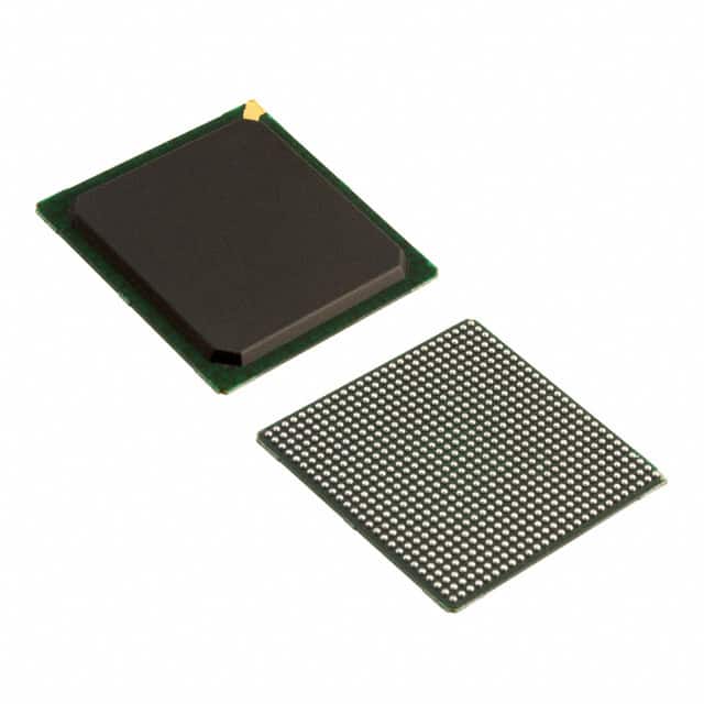
Package
The M1A3PE1500-2FGG676I comes in a compact and durable package, ensuring protection during handling and installation. The package is designed to facilitate easy integration into electronic systems.
Essence
The essence of the M1A3PE1500-2FGG676I lies in its ability to provide a customizable hardware solution for demanding applications. By programming the FPGA, users can tailor its functionality to meet specific requirements, eliminating the need for custom-designed ASICs.
Packaging/Quantity
The M1A3PE1500-2FGG676I is typically packaged individually and is available in varying quantities depending on the customer's needs.
Specifications
- FPGA Family: M1A3PE
- Logic Elements: 1,500,000
- Number of I/O Pins: 676
- Package Type: FGG676
- Operating Temperature Range: -40°C to +85°C
- Supply Voltage: 1.2V
Detailed Pin Configuration
For a detailed pin configuration diagram of the M1A3PE1500-2FGG676I, please refer to the manufacturer's datasheet.
Functional Features
- High-speed data processing capabilities
- Support for various communication protocols
- On-chip memory resources for efficient data storage and retrieval
- Built-in digital signal processing (DSP) blocks for accelerated algorithm execution
- Configurable I/O standards for seamless integration with external devices
Advantages and Disadvantages
Advantages
- Flexibility: The reprogrammable nature of FPGAs allows for quick prototyping and design iterations.
- Performance: FPGAs can handle complex algorithms and large datasets, making them suitable for high-performance applications.
- Cost-effectiveness: By using FPGAs, the need for custom ASIC development can be eliminated, reducing overall costs.
Disadvantages
- Power Consumption: FPGAs tend to consume more power compared to dedicated ASICs.
- Design Complexity: Programming FPGAs requires specialized knowledge and expertise.
- Limited Scalability: FPGAs may have limitations in terms of logic capacity and I/O capabilities compared to ASICs.
Working Principles
FPGAs consist of an array of configurable logic blocks (CLBs) interconnected by programmable routing resources. The M1A3PE1500-2FGG676I utilizes a combination of look-up tables, flip-flops, and interconnect resources to implement desired logic functions. The FPGA is programmed using Hardware Description Languages (HDLs) such as VHDL or Verilog, which describe the desired functionality at a higher level.
Detailed Application Field Plans
The M1A3PE1500-2FGG676I finds applications in various fields, including:
- Telecommunications: FPGAs are used in base stations, routers, and network switches to enable high-speed data processing and protocol handling.
- Aerospace and Defense: FPGAs are utilized in radar systems, avionics, and military communication equipment for their real-time processing capabilities and reliability.
- High-Performance Computing: FPGAs can be integrated into supercomputers and data centers to accelerate specific algorithms and improve overall system performance.
- Industrial Automation: FPGAs are employed in control systems, robotics, and machine vision applications for their ability to handle complex real-time tasks.
Detailed and Complete Alternative Models
M1A2PE1000-2FGG484I
- Logic Elements: 1,000,000
- Number of I/O Pins: 484
- Package Type: FGG484
- Supply Voltage: 1.2V
M1A5PE2000-3FGG900I
- Logic Elements: 2,000,000
- Number of I/O Pins: 900
- Package Type: FGG900
- Supply Voltage: 1.2V
M1A7PE3000-4FGG1156I
- Logic Elements: 3,000,000
- Number of I/O Pins: 1156
10个与M1A3PE1500-2FGG676I在技术解决方案中的应用相关的常见问题及解答
Sure! Here are 10 common questions and answers related to the application of M1A3PE1500-2FGG676I in technical solutions:
Q1: What is M1A3PE1500-2FGG676I? A1: M1A3PE1500-2FGG676I is a specific model of field-programmable gate array (FPGA) that offers high-performance capabilities for various technical applications.
Q2: What are the key features of M1A3PE1500-2FGG676I? A2: Some key features of M1A3PE1500-2FGG676I include a large number of programmable logic cells, high-speed transceivers, embedded memory blocks, and support for various communication protocols.
Q3: What are the typical applications of M1A3PE1500-2FGG676I? A3: M1A3PE1500-2FGG676I can be used in a wide range of applications such as telecommunications, data centers, aerospace, defense systems, industrial automation, and high-performance computing.
Q4: How does M1A3PE1500-2FGG676I enhance performance in technical solutions? A4: M1A3PE1500-2FGG676I enhances performance by providing flexible hardware acceleration, parallel processing capabilities, and the ability to implement complex algorithms efficiently.
Q5: Can M1A3PE1500-2FGG676I be easily integrated into existing systems? A5: Yes, M1A3PE1500-2FGG676I is designed to be easily integrated into existing systems through its standard interfaces and compatibility with industry-standard design tools.
Q6: Does M1A3PE1500-2FGG676I support multiple communication protocols? A6: Yes, M1A3PE1500-2FGG676I supports various communication protocols such as Ethernet, PCIe, USB, and high-speed serial interfaces.
Q7: What are the power requirements for M1A3PE1500-2FGG676I? A7: The power requirements for M1A3PE1500-2FGG676I depend on the specific implementation and configuration. It is recommended to refer to the datasheet or user guide for detailed power specifications.
Q8: Can M1A3PE1500-2FGG676I be reprogrammed after deployment? A8: Yes, M1A3PE1500-2FGG676I is a field-programmable device, which means it can be reprogrammed even after deployment to adapt to changing requirements or to fix bugs.
Q9: Are there any development kits or tools available for M1A3PE1500-2FGG676I? A9: Yes, the manufacturer of M1A3PE1500-2FGG676I provides development kits and tools that enable designers to efficiently develop and test their applications using this FPGA.
Q10: Where can I find technical support or documentation for M1A3PE1500-2FGG676I? A10: Technical support and documentation for M1A3PE1500-2FGG676I can be obtained from the manufacturer's website, which typically includes datasheets, user guides, application notes, and forums for community support.
Please note that the specific details and answers may vary depending on the manufacturer and the specific implementation of M1A3PE1500-2FGG676I.