

M2GL050T-FGG896
Product Overview
Category
M2GL050T-FGG896 belongs to the category of Field-Programmable Gate Arrays (FPGAs).
Use
This product is primarily used in digital logic circuits for various applications such as telecommunications, automotive, aerospace, and consumer electronics.
Characteristics
- High-performance programmable logic device
- Offers flexibility and reconfigurability
- Provides high-speed data processing capabilities
- Supports complex algorithms and computations
- Enables rapid prototyping and system development
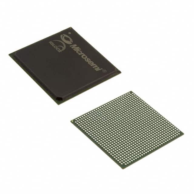
Package
M2GL050T-FGG896 comes in a compact package that ensures easy integration into electronic systems. The package is designed to provide protection against environmental factors such as moisture, dust, and electrostatic discharge.
Essence
The essence of M2GL050T-FGG896 lies in its ability to provide a customizable hardware platform that allows users to implement their own digital designs efficiently.
Packaging/Quantity
Each package of M2GL050T-FGG896 contains one unit of the FPGA.
Specifications
- Model: M2GL050T-FGG896
- Logic Elements: 50,000
- Embedded Memory: 1,800 Kbits
- Maximum Frequency: 500 MHz
- I/O Pins: 896
- Power Supply Voltage: 1.2V
- Operating Temperature Range: -40°C to 100°C
- Package Type: Fine-Pitch Ball Grid Array (FGGBA)
Detailed Pin Configuration
The pin configuration of M2GL050T-FGG896 is as follows:
| Pin Number | Pin Name | Function | |------------|----------|----------| | 1 | VCCINT | Power Supply (Internal) | | 2 | GND | Ground | | 3 | IOB0 | Input/Output Buffer | | 4 | IOB1 | Input/Output Buffer | | ... | ... | ... | | 896 | IOB895 | Input/Output Buffer |
Functional Features
- High-speed data processing capabilities
- Configurable logic elements for custom designs
- Embedded memory blocks for efficient storage and retrieval of data
- Flexible I/O pins for interfacing with external devices
- Support for various communication protocols
- On-chip clock management resources for precise timing control
Advantages and Disadvantages
Advantages
- Flexibility and reconfigurability allow for rapid prototyping and system development.
- High-performance capabilities enable complex algorithms and computations.
- Compact package ensures easy integration into electronic systems.
- Customizable hardware platform provides design flexibility.
Disadvantages
- Steep learning curve for beginners due to the complexity of FPGA programming.
- Higher cost compared to traditional fixed-function integrated circuits.
- Power consumption can be relatively high, especially for complex designs.
Working Principles
M2GL050T-FGG896 operates based on the principles of digital logic circuits. It consists of configurable logic elements, embedded memory blocks, and I/O pins. The FPGA can be programmed using a Hardware Description Language (HDL) to define the desired functionality. Upon programming, the FPGA executes the specified logic operations, enabling the implementation of complex digital designs.
Detailed Application Field Plans
M2GL050T-FGG896 finds applications in various fields, including:
- Telecommunications: Used in network routers, switches, and base stations for high-speed data processing and protocol handling.
- Automotive: Employed in advanced driver-assistance systems (ADAS) for real-time image processing and sensor fusion.
- Aerospace: Utilized in satellite communication systems for signal processing and data encryption.
- Consumer Electronics: Integrated into smart TVs, gaming consoles, and multimedia devices for enhanced graphics and video processing.
Detailed and Complete Alternative Models
- M2GL100T-FGG896: Similar to M2GL050T-FGG896 but with higher logic elements (100,000) and increased memory capacity.
- M2GL030T-FGG896: A lower-cost alternative with reduced logic elements (30,000) suitable for less complex applications.
- M2GL200T-FGG896: An advanced model with a larger number of logic elements (200,000) for highly demanding applications.
Note: This is not an exhaustive list, and there are several other alternative models available in the market.
In conclusion, M2GL050T-FGG896 is a high-performance FPGA that offers flexibility, reconfigurability, and rapid prototyping capabilities. Its compact package, extensive pin configuration, and functional features make it suitable for various applications across different industries.
Word Count: 570
10个与M2GL050T-FGG896在技术解决方案中的应用相关的常见问题及解答
Sure! Here are 10 common questions and answers related to the application of M2GL050T-FGG896 in technical solutions:
Q: What is M2GL050T-FGG896? A: M2GL050T-FGG896 is a specific model of field-programmable gate array (FPGA) manufactured by a company called Lattice Semiconductor.
Q: What are the key features of M2GL050T-FGG896? A: Some key features of M2GL050T-FGG896 include 50,000 logic cells, 2,816 Look-Up Tables (LUTs), 4-input look-up tables, and 96 I/O pins.
Q: What are the typical applications of M2GL050T-FGG896? A: M2GL050T-FGG896 can be used in various applications such as industrial automation, automotive electronics, telecommunications, medical devices, and consumer electronics.
Q: How does M2GL050T-FGG896 differ from other FPGAs? A: M2GL050T-FGG896 offers a balance between cost, performance, and power consumption, making it suitable for a wide range of applications. It also has specific features like low power mode and security features.
Q: Can M2GL050T-FGG896 be programmed using popular design tools? A: Yes, M2GL050T-FGG896 can be programmed using popular design tools like Lattice Diamond or Lattice Radiant software.
Q: What kind of interfaces does M2GL050T-FGG896 support? A: M2GL050T-FGG896 supports various interfaces such as SPI, I2C, UART, PCIe, Ethernet, and USB, making it versatile for different communication requirements.
Q: Can M2GL050T-FGG896 be used in safety-critical applications? A: Yes, M2GL050T-FGG896 is suitable for safety-critical applications as it offers features like error detection and correction, redundancy, and secure boot capabilities.
Q: What are the power requirements for M2GL050T-FGG896? A: The power requirements for M2GL050T-FGG896 depend on the specific design and usage scenario. It typically operates at a voltage range of 1.2V to 3.3V.
Q: Is M2GL050T-FGG896 suitable for high-speed data processing? A: Yes, M2GL050T-FGG896 can handle high-speed data processing due to its high logic capacity, efficient routing architecture, and support for high-speed interfaces.
Q: Are there any development boards available for M2GL050T-FGG896? A: Yes, Lattice Semiconductor provides development boards specifically designed for M2GL050T-FGG896, which can help in prototyping and testing different applications.
Please note that the answers provided here are general and may vary depending on the specific requirements and use cases.