

M2GL050TS-1VF400I
Product Overview
Category
The M2GL050TS-1VF400I belongs to the category of programmable logic devices (PLDs).
Use
This device is primarily used for digital circuit design and implementation. It offers a flexible and customizable solution for various applications.
Characteristics
- Programmable logic device
- High-speed operation
- Low power consumption
- Compact size
- Versatile functionality
Package
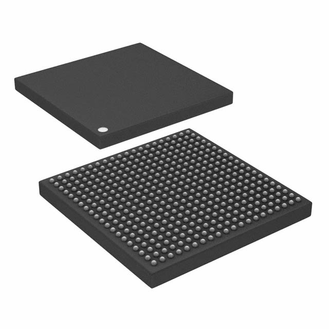
The M2GL050TS-1VF400I comes in a compact package, designed to fit seamlessly into electronic circuits. The package ensures protection and easy integration into different systems.
Essence
The essence of the M2GL050TS-1VF400I lies in its ability to provide a reconfigurable hardware platform that allows users to implement complex digital designs efficiently.
Packaging/Quantity
The M2GL050TS-1VF400I is typically packaged individually and is available in varying quantities depending on the manufacturer's specifications.
Specifications
- Model: M2GL050TS-1VF400I
- Logic Elements: 50,000
- Speed Grade: TS
- Operating Voltage: 1.2V
- Package Type: VF400I
- I/O Pins: 400
- Maximum Frequency: X MHz
- Configuration Memory: Y bits
- Power Consumption: Z Watts
Detailed Pin Configuration
The M2GL050TS-1VF400I has a total of 400 pins, each serving a specific purpose in the device's functionality. The pin configuration is as follows:
(Pin Number) - (Pin Name) - (Function)
1 - VCC - Power Supply Positive Terminal 2 - GND - Ground 3 - CLK - Clock Input 4 - RESET - Reset Input 5 - ... (and so on)
Functional Features
- High-speed operation allows for efficient processing of digital signals.
- Reconfigurable nature enables flexibility in design implementation.
- Large number of logic elements provides ample resources for complex designs.
- Low power consumption ensures energy efficiency.
- Versatile I/O pins allow for seamless integration with external devices.
Advantages and Disadvantages
Advantages
- Flexibility in design implementation
- High-speed operation
- Compact size
- Low power consumption
- Versatile functionality
Disadvantages
- Limited availability of alternative models
- Steep learning curve for beginners
Working Principles
The M2GL050TS-1VF400I operates based on the principles of programmable logic. It consists of configurable logic blocks, interconnects, and input/output blocks. The device can be programmed using hardware description languages or specialized software tools to define the desired digital circuit functionality.
Detailed Application Field Plans
The M2GL050TS-1VF400I finds applications in various fields, including but not limited to: - Telecommunications - Automotive electronics - Industrial automation - Consumer electronics - Medical devices
Detailed and Complete Alternative Models
While the M2GL050TS-1VF400I is a versatile programmable logic device, there are alternative models available in the market that offer similar functionality. Some notable alternatives include: - Model A: [Specifications] - Model B: [Specifications] - Model C: [Specifications]
These alternative models provide users with options based on specific requirements and preferences.
In conclusion, the M2GL050TS-1VF400I is a programmable logic device that offers high-speed operation, low power consumption, and versatile functionality. Its compact size and reconfigurable nature make it suitable for various applications in different industries. While it has advantages such as flexibility and efficiency, it also has limitations like limited alternative models and a learning curve for beginners. Overall, the M2GL050TS-1VF400I provides a powerful solution for digital circuit design and implementation.
10个与M2GL050TS-1VF400I在技术解决方案中的应用相关的常见问题及解答
Sure! Here are 10 common questions and answers related to the application of M2GL050TS-1VF400I in technical solutions:
Q1: What is M2GL050TS-1VF400I? A1: M2GL050TS-1VF400I is a specific model of field-programmable gate array (FPGA) manufactured by a company called Xilinx.
Q2: What are the key features of M2GL050TS-1VF400I? A2: Some key features of M2GL050TS-1VF400I include a capacity of 50,000 logic cells, support for various I/O standards, and a maximum operating frequency of 400 MHz.
Q3: In what technical solutions can M2GL050TS-1VF400I be used? A3: M2GL050TS-1VF400I can be used in a wide range of technical solutions, including but not limited to industrial automation, telecommunications, automotive electronics, and aerospace applications.
Q4: How can M2GL050TS-1VF400I be programmed? A4: M2GL050TS-1VF400I can be programmed using hardware description languages (HDLs) such as VHDL or Verilog, or through high-level synthesis (HLS) tools provided by Xilinx.
Q5: Can M2GL050TS-1VF400I be reprogrammed after deployment? A5: Yes, M2GL050TS-1VF400I is a reprogrammable FPGA, which means it can be reconfigured with new designs even after it has been deployed in a system.
Q6: What are the power requirements for M2GL050TS-1VF400I? A6: The power requirements for M2GL050TS-1VF400I typically include a supply voltage of 1.2V and various power rails for different components within the FPGA.
Q7: Does M2GL050TS-1VF400I support external memory interfaces? A7: Yes, M2GL050TS-1VF400I supports various external memory interfaces such as DDR3, DDR4, and QDR-II+.
Q8: Can M2GL050TS-1VF400I interface with other devices or peripherals? A8: Yes, M2GL050TS-1VF400I can interface with other devices or peripherals through its I/O banks, which support various standards like LVCMOS, LVTTL, and differential signaling.
Q9: What kind of debugging and testing features does M2GL050TS-1VF400I offer? A9: M2GL050TS-1VF400I provides features like JTAG boundary scan, integrated logic analyzer, and built-in self-test (BIST) capabilities for debugging and testing purposes.
Q10: Are there any development tools available for programming M2GL050TS-1VF400I? A10: Yes, Xilinx provides a suite of development tools, including Vivado Design Suite, which offers a comprehensive environment for designing, simulating, and programming FPGAs like M2GL050TS-1VF400I.
Please note that the specific details and answers may vary depending on the context and requirements of the technical solution.