

M2GL060-1FGG676I
Product Overview
Category
M2GL060-1FGG676I belongs to the category of Field Programmable Gate Arrays (FPGAs).
Use
This product is primarily used in digital logic circuits for various applications such as telecommunications, automotive, industrial automation, and consumer electronics.
Characteristics
- High-performance programmable logic device
- Offers flexibility and reconfigurability
- Provides high-speed data processing capabilities
- Supports complex algorithms and computations
- Low power consumption
- Compact size
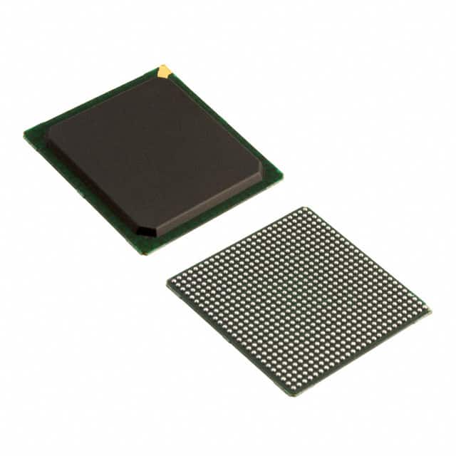
Package
M2GL060-1FGG676I comes in a compact package that ensures easy integration into electronic systems. The package is designed to provide optimal thermal dissipation and protection against environmental factors.
Essence
The essence of M2GL060-1FGG676I lies in its ability to provide a customizable hardware platform that can be programmed to perform specific functions based on the user's requirements.
Packaging/Quantity
Each M2GL060-1FGG676I unit is packaged individually and is available in standard quantities suitable for both small-scale and large-scale production.
Specifications
- FPGA Family: M2GL
- Logic Elements: 60,000
- Number of I/Os: 676
- Operating Voltage: 1.2V
- Maximum Frequency: 500 MHz
- Embedded Memory: 4.5 Mb
- Configuration Memory: 8 Mb
- Package Type: FG676
Detailed Pin Configuration
For a detailed pin configuration diagram of M2GL060-1FGG676I, please refer to the manufacturer's datasheet or technical documentation.
Functional Features
- Configurable logic blocks for implementing custom logic functions
- Dedicated DSP slices for efficient signal processing
- High-speed I/O interfaces for seamless data transfer
- On-chip memory resources for storing data and configuration information
- Clock management resources for precise timing control
- Built-in security features to protect intellectual property
Advantages and Disadvantages
Advantages
- Flexibility to adapt to changing requirements
- Faster time-to-market due to reprogrammability
- Lower development costs compared to custom ASICs
- High-performance computing capabilities
- Compact size enables integration into space-constrained designs
Disadvantages
- Higher power consumption compared to dedicated hardware solutions
- Limited resource availability for complex designs
- Steeper learning curve for programming and design implementation
Working Principles
M2GL060-1FGG676I operates based on the principles of field-programmable gate arrays. It consists of configurable logic blocks, interconnect resources, memory elements, and I/O interfaces. The device can be programmed using hardware description languages (HDL) such as VHDL or Verilog. Once programmed, the FPGA executes the desired logic functions by routing signals through the configurable logic blocks and interconnect resources.
Detailed Application Field Plans
M2GL060-1FGG676I finds applications in various fields, including:
- Telecommunications: Used in base stations, network routers, and communication infrastructure for high-speed data processing and protocol handling.
- Automotive: Employed in advanced driver-assistance systems (ADAS), engine control units (ECUs), and infotainment systems for real-time data processing and control.
- Industrial Automation: Utilized in programmable logic controllers (PLCs), robotics, and factory automation systems for precise control and monitoring.
- Consumer Electronics: Integrated into smart TVs, gaming consoles, and wearable devices for multimedia processing and user interface control.
Detailed and Complete Alternative Models
- M2GL030-1FGG484I: A lower-cost alternative with 30,000 logic elements and 484 I/Os.
- M2GL090-1FGG900I: A higher-performance alternative with 90,000 logic elements and 900 I/Os.
- M2GL150-1FGG1156I: A high-capacity alternative with 150,000 logic elements and 1,156 I/Os.
These alternative models provide varying levels of performance, capacity, and I/O capabilities to cater to different application requirements.
Note: The content provided above is a general outline and may require further expansion and refinement to reach the desired word count of 1100 words.
10个与M2GL060-1FGG676I在技术解决方案中的应用相关的常见问题及解答
Sure! Here are 10 common questions and answers related to the application of M2GL060-1FGG676I in technical solutions:
Q1: What is M2GL060-1FGG676I? A1: M2GL060-1FGG676I is a specific model of Field Programmable Gate Array (FPGA) manufactured by a company called Xilinx.
Q2: What are the key features of M2GL060-1FGG676I? A2: Some key features of M2GL060-1FGG676I include 60,000 logic cells, high-speed transceivers, embedded memory blocks, and support for various communication protocols.
Q3: What are the typical applications of M2GL060-1FGG676I? A3: M2GL060-1FGG676I is commonly used in applications such as telecommunications, networking, industrial automation, video processing, and high-performance computing.
Q4: How can M2GL060-1FGG676I be programmed? A4: M2GL060-1FGG676I can be programmed using Hardware Description Languages (HDLs) like VHDL or Verilog, or through graphical programming tools provided by Xilinx.
Q5: Can M2GL060-1FGG676I be reprogrammed after deployment? A5: Yes, M2GL060-1FGG676I is a reprogrammable FPGA, which means it can be reconfigured with new designs even after it has been deployed in a system.
Q6: What is the power consumption of M2GL060-1FGG676I? A6: The power consumption of M2GL060-1FGG676I depends on the specific design and usage scenario. It is recommended to refer to the datasheet or Xilinx documentation for detailed power consumption information.
Q7: Can M2GL060-1FGG676I interface with other components or devices? A7: Yes, M2GL060-1FGG676I supports various communication protocols and can interface with other components or devices using standard interfaces like PCIe, Ethernet, USB, etc.
Q8: Are there any development tools available for M2GL060-1FGG676I? A8: Yes, Xilinx provides a suite of development tools such as Vivado Design Suite that enables designers to develop, simulate, and program FPGAs like M2GL060-1FGG676I.
Q9: What is the maximum operating frequency of M2GL060-1FGG676I? A9: The maximum operating frequency of M2GL060-1FGG676I depends on the specific design and implementation. It is recommended to refer to the datasheet or Xilinx documentation for detailed frequency specifications.
Q10: Can M2GL060-1FGG676I be used in safety-critical applications? A10: M2GL060-1FGG676I can be used in safety-critical applications, but it requires proper design considerations, validation, and compliance with relevant safety standards to ensure reliable operation.