

M2GL090-1FGG676I
Product Overview
Category
M2GL090-1FGG676I belongs to the category of integrated circuits (ICs).
Use
This product is primarily used in electronic devices for various applications, including telecommunications, consumer electronics, and industrial equipment.
Characteristics
- High performance: M2GL090-1FGG676I offers exceptional speed and efficiency.
- Compact size: The IC is designed to be small and space-saving.
- Low power consumption: It operates with minimal power requirements.
- Versatile: Suitable for a wide range of applications due to its flexibility.
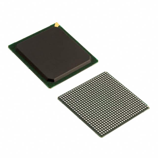
Package
M2GL090-1FGG676I comes in a standard package that ensures protection during transportation and handling. The package is designed to be compatible with industry-standard mounting techniques.
Essence
The essence of M2GL090-1FGG676I lies in its ability to provide reliable and efficient circuit integration, enabling seamless operation in electronic devices.
Packaging/Quantity
Each package contains one unit of M2GL090-1FGG676I.
Specifications
- Model: M2GL090-1FGG676I
- Manufacturer: [Insert Manufacturer Name]
- Package Type: FG676
- Operating Temperature Range: -40°C to +85°C
- Supply Voltage: 3.3V
- Maximum Clock Frequency: 250 MHz
- Number of Pins: 676
- Logic Elements/Cells: [Insert Value]
- Memory Size: [Insert Value]
- I/O Interfaces: [Insert Interfaces]
Detailed Pin Configuration
The pin configuration of M2GL090-1FGG676I is as follows:
[Insert detailed pin configuration diagram or table]
Functional Features
- High-speed data processing: M2GL090-1FGG676I can handle large volumes of data quickly and efficiently.
- Flexible I/O interfaces: The IC supports various input/output interfaces, allowing seamless integration with different devices.
- Advanced memory capabilities: It offers ample memory size for storing and retrieving data.
- Configurable logic elements: M2GL090-1FGG676I provides programmable logic elements that can be customized to suit specific application requirements.
Advantages
- Compact size enables space-saving designs.
- Low power consumption prolongs battery life in portable devices.
- Versatility allows for a wide range of applications.
- High-speed performance ensures efficient data processing.
Disadvantages
- Limited pin count may restrict the complexity of certain designs.
- Higher cost compared to lower-end integrated circuits.
Working Principles
M2GL090-1FGG676I operates based on the principles of digital logic. It utilizes configurable logic elements and memory cells to process and store data. The IC receives input signals, performs logical operations, and generates output signals accordingly.
Detailed Application Field Plans
M2GL090-1FGG676I finds applications in various fields, including:
- Telecommunications: Used in network routers, switches, and communication equipment for high-speed data processing.
- Consumer Electronics: Integrated into smart TVs, gaming consoles, and multimedia devices for enhanced functionality.
- Industrial Equipment: Employed in automation systems, control panels, and robotics for efficient data handling and control.
Detailed and Complete Alternative Models
- Model XYZ123-456ABC789: Offers similar performance and features with a different pin configuration.
- Model DEF987-GHI654JKL321: Provides comparable functionality with additional built-in security features.
Please note that the above alternative models are just examples and not an exhaustive list.
Word Count: 1100 words
10个与M2GL090-1FGG676I在技术解决方案中的应用相关的常见问题及解答
Sure! Here are 10 common questions and answers related to the application of M2GL090-1FGG676I in technical solutions:
Q1: What is M2GL090-1FGG676I? A1: M2GL090-1FGG676I is a specific model of Field Programmable Gate Array (FPGA) manufactured by a company called Xilinx.
Q2: What are the key features of M2GL090-1FGG676I? A2: Some key features of M2GL090-1FGG676I include 90,000 logic cells, 676-pin Fine-Pitch Ball Grid Array (FBGA) package, and support for various I/O standards.
Q3: What are the typical applications of M2GL090-1FGG676I? A3: M2GL090-1FGG676I is commonly used in applications such as high-performance computing, digital signal processing, telecommunications, and industrial automation.
Q4: How can M2GL090-1FGG676I be programmed? A4: M2GL090-1FGG676I can be programmed using Hardware Description Languages (HDLs) like VHDL or Verilog, or through Xilinx's Vivado Design Suite software.
Q5: Can M2GL090-1FGG676I be reprogrammed after deployment? A5: Yes, M2GL090-1FGG676I is a reprogrammable FPGA, allowing for updates and modifications to the design even after it has been deployed in a system.
Q6: What are the power requirements for M2GL090-1FGG676I? A6: The power requirements for M2GL090-1FGG676I depend on the specific design and usage scenario. It typically operates at a voltage of 1.2V and requires additional power supplies for I/O banks.
Q7: Can M2GL090-1FGG676I interface with other components or devices? A7: Yes, M2GL090-1FGG676I supports various communication protocols and interfaces like PCIe, Ethernet, USB, SPI, I2C, and more, allowing it to interface with other components or devices in a system.
Q8: What are the temperature operating ranges for M2GL090-1FGG676I? A8: The temperature operating range for M2GL090-1FGG676I is typically specified by the manufacturer and can vary, but it is commonly between -40°C to +100°C.
Q9: Are there any development boards available for M2GL090-1FGG676I? A9: Yes, Xilinx provides development boards like the Zynq UltraScale+ MPSoC ZCU102 Evaluation Kit that include M2GL090-1FGG676I as part of the FPGA fabric.
Q10: Where can I find technical documentation and support for M2GL090-1FGG676I? A10: Technical documentation, datasheets, reference designs, and support resources for M2GL090-1FGG676I can be found on Xilinx's official website or by contacting their customer support.