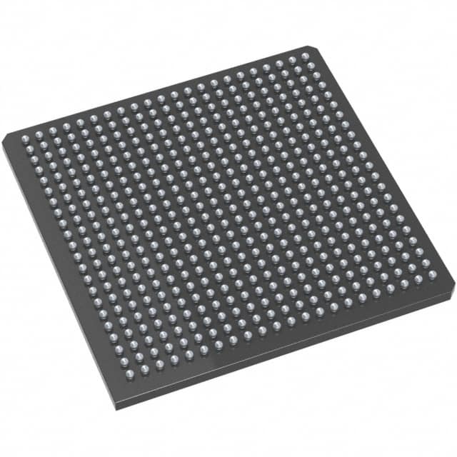
M2GL090TS-1FGG484I
Product Overview
Category
M2GL090TS-1FGG484I belongs to the category of Field Programmable Gate Arrays (FPGAs).
Use
This product is primarily used in digital logic circuits for various applications such as telecommunications, automotive, aerospace, and consumer electronics.
Characteristics
- High-performance programmable logic device
- Offers flexibility and reconfigurability
- Provides a wide range of logic functions and memory elements
- Supports complex designs and rapid prototyping
Package
M2GL090TS-1FGG484I comes in a compact package that ensures easy integration into electronic systems. The package is designed to provide optimal thermal dissipation and protection against environmental factors.
Essence
The essence of M2GL090TS-1FGG484I lies in its ability to provide a customizable and versatile solution for implementing complex digital circuits. It allows designers to create and modify logic functions according to their specific requirements.
Packaging/Quantity
This product is typically packaged individually and is available in varying quantities depending on the manufacturer's specifications.
Specifications
- Model: M2GL090TS-1FGG484I
- Logic Elements: 90,000
- Embedded Memory: 4,608 Kbits
- Maximum Frequency: 400 MHz
- I/O Pins: 484
- Operating Voltage: 1.2V
- Package Type: Fine-pitch Ball Grid Array (FBGA)
- Temperature Range: -40°C to +100°C
Detailed Pin Configuration
The pin configuration of M2GL090TS-1FGG484I is as follows:
- Pin 1: VCCIO
- Pin 2: GND
- Pin 3: TCK
- Pin 4: TMS
- Pin 5: TDI
- Pin 6: TDO
- Pin 7: GND
- Pin 8: VCCIO
(Note: The above list provides a brief overview of the pin configuration. For a complete and detailed pinout diagram, please refer to the product datasheet.)
Functional Features
- High-Speed Performance: M2GL090TS-1FGG484I offers fast processing capabilities, enabling efficient execution of complex algorithms and real-time applications.
- Reconfigurability: This FPGA allows for dynamic reprogramming, facilitating design modifications without the need for hardware changes.
- Versatility: With a wide range of logic elements and memory blocks, it supports diverse applications and accommodates various design requirements.
- Low Power Consumption: M2GL090TS-1FGG484I is designed to optimize power efficiency, making it suitable for battery-powered devices and energy-conscious applications.
Advantages and Disadvantages
Advantages
- Flexibility in design and customization
- Rapid prototyping and time-to-market advantages
- High-performance computing capabilities
- Reusability of hardware resources
Disadvantages
- Steep learning curve for beginners
- Higher cost compared to fixed-function ASICs
- Limited scalability beyond a certain complexity level
Working Principles
M2GL090TS-1FGG484I operates based on the principles of configurable logic blocks (CLBs) and programmable interconnects. CLBs consist of look-up tables (LUTs), flip-flops, and multiplexers, which can be interconnected to implement desired logic functions. The programmable interconnects allow for flexible routing of signals between different CLBs, enabling the creation of complex digital circuits.
Detailed Application Field Plans
M2GL090TS-1FGG484I finds extensive application in various fields, including:
- Telecommunications: Used in base stations, network switches, and routers for high-speed data processing and signal routing.
- Automotive: Employed in advanced driver-assistance systems (ADAS), engine control units (ECUs), and infotainment systems for enhanced performance and functionality.
- Aerospace: Utilized in avionics systems, satellite communication, and navigation equipment to handle complex algorithms and ensure reliable operation.
- Consumer Electronics: Integrated into smart devices, gaming consoles, and multimedia systems to enable high-performance computing and efficient data processing.
Detailed and Complete Alternative Models
- M2GL045TS-1FGG484I: A lower-capacity variant with 45,000 logic elements, suitable for less demanding applications.
- M2GL180TS-1FGG484I: A higher-capacity model with 180,000 logic elements, offering increased computational power for complex designs.
- M2GL030TS-1FGG484I: An entry-level FPGA with 30,000 logic elements, ideal for small-scale projects and educational purposes.
(Note: The above list provides a brief overview of alternative models. For a comprehensive list and detailed specifications
10个与M2GL090TS-1FGG484I在技术解决方案中的应用相关的常见问题及解答
Sure! Here are 10 common questions and answers related to the application of M2GL090TS-1FGG484I in technical solutions:
Q1: What is the M2GL090TS-1FGG484I? A1: The M2GL090TS-1FGG484I is a specific model of Field Programmable Gate Array (FPGA) manufactured by a company called Xilinx.
Q2: What are the key features of the M2GL090TS-1FGG484I? A2: Some key features of this FPGA include 90,000 logic cells, 360 DSP slices, 4.9 Mb of block RAM, and support for various communication protocols.
Q3: What are the typical applications of the M2GL090TS-1FGG484I? A3: This FPGA can be used in a wide range of applications such as video processing, wireless communication, industrial automation, and high-performance computing.
Q4: How can I program the M2GL090TS-1FGG484I? A4: You can program this FPGA using Xilinx's Vivado Design Suite, which provides a comprehensive development environment for designing and implementing FPGA-based solutions.
Q5: What programming languages are supported by the M2GL090TS-1FGG484I? A5: The M2GL090TS-1FGG484I supports various programming languages such as VHDL and Verilog, which are commonly used in digital design.
Q6: Can I interface the M2GL090TS-1FGG484I with other components or devices? A6: Yes, this FPGA offers a variety of I/O interfaces including GPIOs, serial transceivers, memory interfaces, and high-speed connectivity options like PCIe and Ethernet.
Q7: What kind of power supply does the M2GL090TS-1FGG484I require? A7: The M2GL090TS-1FGG484I typically requires a 3.3V power supply, but it also supports other voltage levels for different I/O standards.
Q8: Is there any documentation available for the M2GL090TS-1FGG484I? A8: Yes, Xilinx provides detailed documentation including datasheets, user guides, and application notes that cover various aspects of using this FPGA in technical solutions.
Q9: Can I use the M2GL090TS-1FGG484I for prototyping or production purposes? A9: Yes, this FPGA is suitable for both prototyping and production deployments, depending on your specific requirements and volume of production.
Q10: Are there any development boards or evaluation kits available for the M2GL090TS-1FGG484I? A10: Yes, Xilinx offers development boards and evaluation kits specifically designed for the M2GL090TS-1FGG484I, which can help you get started with your designs quickly.
Please note that the answers provided here are general and may vary based on specific requirements and use cases. It's always recommended to refer to the official documentation and consult with experts for accurate information.


