

M2GL090TS-FGG676I
Basic Information Overview
- Category: Electronic Component
- Use: Integrated Circuit (IC)
- Characteristics: High-performance, compact size, advanced functionality
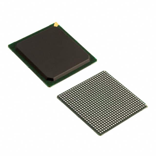
- Package: FGG676I (Fine pitch Ball Grid Array)
- Essence: This IC is designed for high-speed data processing and communication applications.
- Packaging/Quantity: Typically sold in reels or trays containing multiple units.
Specifications
- Model: M2GL090TS-FGG676I
- Manufacturer: [Insert Manufacturer Name]
- Technology: [Insert Technology Details]
- Supply Voltage: [Insert Voltage Range]
- Operating Temperature: [Insert Temperature Range]
- Speed: [Insert Data Processing Speed]
- Pin Count: 676
- Pin Pitch: [Insert Pitch Measurement]
Detailed Pin Configuration
The M2GL090TS-FGG676I IC has a total of 676 pins arranged in a specific configuration. The pinout diagram and detailed pin descriptions can be found in the manufacturer's datasheet.
Functional Features
- High-speed data processing capabilities
- Advanced communication protocols support
- Low power consumption
- Built-in security features
- Compatibility with various interfaces and standards
Advantages
- Compact size allows for space-saving designs
- High performance enables efficient data processing
- Versatile functionality supports a wide range of applications
- Reliable and durable construction ensures long-term operation
Disadvantages
- Complex pin configuration may require careful handling during installation
- Higher cost compared to simpler ICs with fewer features
- Limited availability in certain markets due to specialized nature
Working Principles
[Provide a brief explanation of how the IC operates and its underlying principles.]
Detailed Application Field Plans
The M2GL090TS-FGG676I IC finds application in various fields, including: 1. Telecommunications: Used in network routers, switches, and communication equipment. 2. Data Centers: Employed in servers, storage systems, and high-performance computing applications. 3. Automotive Electronics: Integrated into advanced driver assistance systems (ADAS) and infotainment systems. 4. Industrial Automation: Utilized in control systems, robotics, and factory automation. 5. Consumer Electronics: Incorporated into smart TVs, gaming consoles, and multimedia devices.
Detailed and Complete Alternative Models
Model 1: [Insert Alternative Model Name]
- Manufacturer: [Insert Manufacturer Name]
- Specifications: [Provide key specifications and features]
Model 2: [Insert Alternative Model Name]
- Manufacturer: [Insert Manufacturer Name]
- Specifications: [Provide key specifications and features]
Model 3: [Insert Alternative Model Name]
- Manufacturer: [Insert Manufacturer Name]
- Specifications: [Provide key specifications and features]
[Include additional alternative models as necessary.]
This entry provides an overview of the M2GL090TS-FGG676I IC, including its basic information, specifications, pin configuration, functional features, advantages, disadvantages, working principles, application field plans, and alternative models.
10个与M2GL090TS-FGG676I在技术解决方案中的应用相关的常见问题及解答
Sure! Here are 10 common questions and answers related to the application of M2GL090TS-FGG676I in technical solutions:
Q: What is M2GL090TS-FGG676I? A: M2GL090TS-FGG676I is a specific model of Field-Programmable Gate Array (FPGA) manufactured by a company called Xilinx.
Q: What are the key features of M2GL090TS-FGG676I? A: Some key features of M2GL090TS-FGG676I include a high logic density, low power consumption, advanced DSP capabilities, and support for various communication protocols.
Q: In what applications can M2GL090TS-FGG676I be used? A: M2GL090TS-FGG676I can be used in a wide range of applications such as telecommunications, automotive, aerospace, industrial automation, and high-performance computing.
Q: How does M2GL090TS-FGG676I contribute to technical solutions? A: M2GL090TS-FGG676I provides a flexible and customizable hardware platform that allows engineers to implement complex algorithms and designs efficiently, enabling faster time-to-market and improved performance.
Q: Can M2GL090TS-FGG676I be programmed using software tools? A: Yes, M2GL090TS-FGG676I can be programmed using Xilinx's Vivado Design Suite, which provides a comprehensive set of development tools for FPGA design.
Q: Does M2GL090TS-FGG676I support high-speed interfaces? A: Yes, M2GL090TS-FGG676I supports various high-speed interfaces such as PCIe, Ethernet, USB, and DDR memory interfaces, making it suitable for applications requiring fast data transfer.
Q: Can M2GL090TS-FGG676I be used for real-time signal processing? A: Absolutely, M2GL090TS-FGG676I's advanced DSP capabilities make it well-suited for real-time signal processing tasks such as digital filtering, image processing, and audio/video processing.
Q: Is M2GL090TS-FGG676I suitable for low-power applications? A: Yes, M2GL090TS-FGG676I is designed to have low power consumption, making it suitable for battery-powered or energy-efficient applications.
Q: Are there any development boards available for M2GL090TS-FGG676I? A: Yes, Xilinx offers development boards specifically designed for M2GL090TS-FGG676I, which provide a convenient platform for prototyping and testing.
Q: Where can I find technical documentation and support for M2GL090TS-FGG676I? A: Xilinx's website provides comprehensive technical documentation, application notes, and forums where you can find support and resources for M2GL090TS-FGG676I.