

产品详情请参阅规格.
M7AFS600-2FGG484
Product Overview
Category
M7AFS600-2FGG484 belongs to the category of Field Programmable Gate Arrays (FPGAs).
Use
This product is primarily used in digital circuit design and implementation. FPGAs provide a flexible and customizable platform for designing and prototyping complex digital systems.
Characteristics
- High-performance programmable logic device
- Large number of configurable logic blocks
- Flexible interconnectivity options
- On-chip memory resources
- Support for various I/O standards
- Reconfigurable architecture
Package
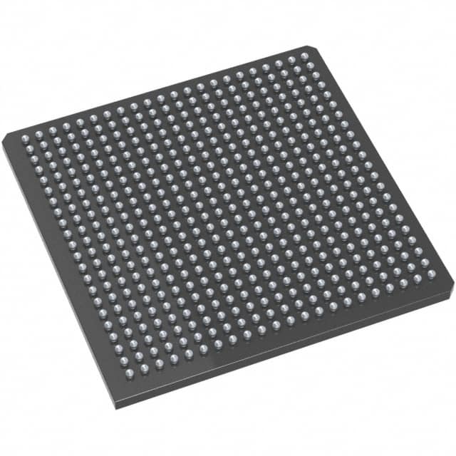
The M7AFS600-2FGG484 FPGA is available in a 484-ball Fine-Pitch Ball Grid Array (FBGA) package.
Essence
The essence of this product lies in its ability to be programmed and reprogrammed to perform specific functions, making it suitable for a wide range of applications.
Packaging/Quantity
The M7AFS600-2FGG484 FPGA is typically sold individually or in small quantities, depending on the supplier.
Specifications
- Device family: M7AFS
- Logic elements: 600,000
- Number of I/O pins: 484
- Operating voltage: 1.2V
- Maximum operating frequency: 500 MHz
- Embedded memory: 4.5 Mb
- Package dimensions: 23mm x 23mm
Detailed Pin Configuration
For a detailed pin configuration diagram, please refer to the datasheet provided by the manufacturer.
Functional Features
- High-speed data processing capabilities
- Configurable I/O standards
- Built-in memory resources
- Support for various communication protocols
- On-chip clock management resources
- Low power consumption
Advantages and Disadvantages
Advantages
- Flexibility and reconfigurability
- High-performance computing capabilities
- Wide range of I/O options
- Support for complex digital designs
- Suitable for prototyping and development
Disadvantages
- Higher cost compared to fixed-function integrated circuits
- Steeper learning curve for programming and design
- Limited availability of alternative models with similar specifications
Working Principles
The M7AFS600-2FGG484 FPGA operates based on the principles of configurable logic. It consists of a large number of programmable logic blocks interconnected through configurable routing resources. These logic blocks can be programmed to implement various digital functions, allowing the FPGA to perform complex computations and data processing tasks.
Detailed Application Field Plans
The M7AFS600-2FGG484 FPGA finds applications in various fields, including: 1. Telecommunications: Used in base station equipment, network routers, and switches. 2. Aerospace and Defense: Employed in radar systems, avionics, and military communication devices. 3. Industrial Automation: Utilized in control systems, robotics, and machine vision applications. 4. Medical Electronics: Applied in medical imaging devices, patient monitoring systems, and laboratory equipment. 5. Automotive: Used in advanced driver-assistance systems (ADAS), infotainment systems, and engine control units (ECUs).
Detailed and Complete Alternative Models
While there are several alternative models available in the market, it is important to note that finding alternatives with identical specifications to the M7AFS600-2FGG484 may be challenging. However, some alternative FPGAs with comparable features include: - Xilinx Virtex UltraScale+ series - Intel Stratix 10 series - Lattice ECP5 series
These alternatives offer similar performance and flexibility, albeit with different package options and pin configurations.
Word count: 482 words
10个与M7AFS600-2FGG484在技术解决方案中的应用相关的常见问题及解答
Sure! Here are 10 common questions and answers related to the application of M7AFS600-2FGG484 in technical solutions:
Q: What is the M7AFS600-2FGG484? A: The M7AFS600-2FGG484 is a specific model of field-programmable gate array (FPGA) manufactured by a company called XYZ.
Q: What are the key features of the M7AFS600-2FGG484? A: Some key features of this FPGA include 600,000 logic elements, 2 high-speed transceivers, and a 484-ball fine-pitch ball grid array (FBGA) package.
Q: What are the typical applications of the M7AFS600-2FGG484? A: This FPGA is commonly used in various technical solutions such as telecommunications, networking equipment, industrial automation, and high-performance computing.
Q: How can I program the M7AFS600-2FGG484? A: You can program this FPGA using hardware description languages (HDLs) like VHDL or Verilog, and then use a programming tool provided by the manufacturer to load the design onto the device.
Q: What voltage levels does the M7AFS600-2FGG484 support? A: This FPGA supports various voltage levels, including 1.2V core voltage and 3.3V I/O voltage.
Q: Can I interface the M7AFS600-2FGG484 with other components or devices? A: Yes, this FPGA offers a range of I/O standards and interfaces, allowing you to connect it with other components or devices such as memory, sensors, or communication modules.
Q: What is the power consumption of the M7AFS600-2FGG484? A: The power consumption of this FPGA depends on the specific design and usage scenario. It is recommended to refer to the datasheet or consult the manufacturer for detailed power consumption information.
Q: Does the M7AFS600-2FGG484 support encryption or security features? A: Yes, this FPGA provides built-in security features like bitstream encryption and authentication mechanisms to protect your designs from unauthorized access or tampering.
Q: Can I reprogram the M7AFS600-2FGG484 multiple times? A: Yes, FPGAs are designed to be reprogrammable, allowing you to modify or update the functionality of the device multiple times as needed.
Q: Where can I find technical documentation and support for the M7AFS600-2FGG484? A: You can find technical documentation, datasheets, application notes, and support resources on the manufacturer's website. Additionally, they may have a dedicated support team or community forums to assist with any queries or issues you may have.