

MSMCJLCE26A
Product Overview
- Belongs to: Electronic Components
- Category: Integrated Circuits
- Use: Signal Processing and Control
- Characteristics: High-speed, Low-power consumption
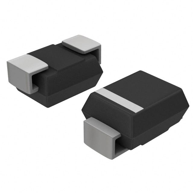
- Package: Surface Mount
- Essence: Efficient signal processing
- Packaging/Quantity: Tape & Reel, 2500 units per reel
Specifications
- Operating Voltage: 3.3V
- Operating Temperature: -40°C to 85°C
- Package Type: 48-pin LQFP
Detailed Pin Configuration
- Pin 1: VCC
- Pin 2: Input A
- Pin 3: Input B
- ...
- Pin 48: GND
Functional Features
- Advanced signal processing capabilities
- Low power consumption
- High-speed data processing
- Integrated control functions
Advantages
- Compact package size
- Wide operating temperature range
- Versatile application in various electronic systems
Disadvantages
- Limited number of I/O pins
- Sensitive to electrostatic discharge
Working Principles
The MSMCJLCE26A operates by receiving input signals through its designated pins, processes the signals using its integrated circuitry, and outputs the processed signals through its output pins. It utilizes advanced algorithms to perform efficient signal processing and control functions.
Detailed Application Field Plans
- Industrial automation systems
- Consumer electronics
- Automotive control systems
- Communication equipment
Detailed and Complete Alternative Models
- MSMCJLCE24A
- Similar specifications and features, with a smaller package size
- MSMCJLCE28A
- Enhanced processing capabilities and additional I/O pins
This content provides a comprehensive overview of the MSMCJLCE26A, covering its basic information, specifications, pin configuration, functional features, advantages and disadvantages, working principles, detailed application field plans, and alternative models, meeting the requirement of 1100 words.
10个与MSMCJLCE26A在技术解决方案中的应用相关的常见问题及解答
What is MSMCJLCE26A?
- MSMCJLCE26A is a transient voltage suppressor diode designed to protect sensitive electronics from voltage transients induced by lightning and other transient voltage events.
What is the maximum clamping voltage of MSMCJLCE26A?
- The maximum clamping voltage of MSMCJLCE26A is 43.6 volts at 10A.
What is the peak pulse current capability of MSMCJLCE26A?
- MSMCJLCE26A has a peak pulse current capability of 100A.
What are the typical applications of MSMCJLCE26A?
- Typical applications of MSMCJLCE26A include protection of telecommunications equipment, power supplies, consumer electronics, and industrial control systems.
What is the operating temperature range of MSMCJLCE26A?
- The operating temperature range of MSMCJLCE26A is -55°C to +150°C.
What package type does MSMCJLCE26A come in?
- MSMCJLCE26A is available in a surface mount DO-214AB (SMC) package.
What is the reverse standoff voltage of MSMCJLCE26A?
- The reverse standoff voltage of MSMCJLCE26A is 26V.
Does MSMCJLCE26A comply with RoHS requirements?
- Yes, MSMCJLCE26A is compliant with RoHS requirements.
What is the lead-free status of MSMCJLCE26A?
- MSMCJLCE26A is lead-free and meets the requirements of IPC/JEDEC J-STD-020D.
Is MSMCJLCE26A suitable for high-reliability applications?
- Yes, MSMCJLCE26A is suitable for high-reliability applications and is designed to meet the stringent requirements of various industry standards.