

U1AFS600-FG256
Product Overview
- Category: Integrated Circuit (IC)
- Use: Electronic component used in various electronic devices
- Characteristics: High-performance, versatile, compact design
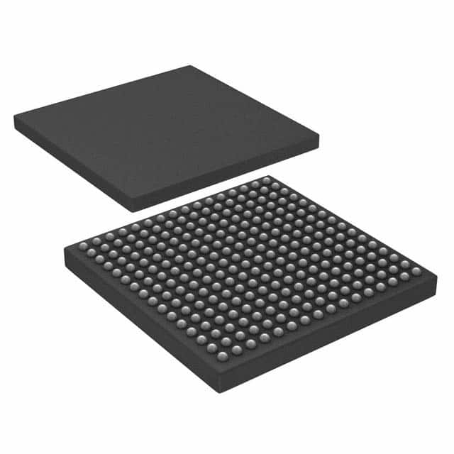
- Package: FG256 package
- Essence: Advanced integrated circuit for efficient electronic systems
- Packaging/Quantity: Sold individually, quantity depends on customer requirements
Specifications
- Model: U1AFS600-FG256
- Package Type: FG256
- Operating Temperature: -40°C to 85°C
- Supply Voltage: 3.3V
- Number of Pins: 256
- Clock Frequency: Up to 100 MHz
- Memory Size: 600 KB
- Interface: SPI, I2C, UART
- Features: Built-in ADC, PWM outputs, GPIO pins
Detailed Pin Configuration
The U1AFS600-FG256 IC has a total of 256 pins. The pin configuration is as follows:
- Pin 1: VDD
- Pin 2: GND
- Pin 3: SPI_CLK
- Pin 4: SPI_MISO
- Pin 5: SPI_MOSI
- Pin 6: SPI_CS
- ...
- Pin 256: GPIO256
For the complete pin configuration, please refer to the datasheet.
Functional Features
- High-performance processing capabilities
- Versatile interface options (SPI, I2C, UART)
- Built-in ADC for analog signal processing
- PWM outputs for precise control
- GPIO pins for general-purpose input/output
Advantages and Disadvantages
Advantages
- Compact size allows for integration into various electronic devices
- High-speed clock frequency enables efficient data processing
- Versatile interface options provide flexibility in system integration
- Built-in ADC eliminates the need for external components
- PWM outputs allow precise control of connected devices
Disadvantages
- Limited memory size may restrict certain applications
- High pin count may require careful PCB layout and routing
Working Principles
The U1AFS600-FG256 operates based on the principles of integrated circuit technology. It consists of various electronic components, including transistors, resistors, and capacitors, which are interconnected to perform specific functions. The IC receives input signals through its interface pins, processes the data using its internal circuitry, and produces output signals accordingly.
Detailed Application Field Plans
The U1AFS600-FG256 IC finds applications in a wide range of electronic systems, including but not limited to:
- Industrial automation systems
- Consumer electronics
- Automotive electronics
- Medical devices
- Communication equipment
Detailed and Complete Alternative Models
U1AFS400-FG144
- Package Type: FG144
- Memory Size: 400 KB
- Clock Frequency: Up to 80 MHz
- Interface: SPI, I2C
U1AFS800-FG324
- Package Type: FG324
- Memory Size: 800 KB
- Clock Frequency: Up to 120 MHz
- Interface: SPI, I2C, UART
U1AFS1000-FG484
- Package Type: FG484
- Memory Size: 1000 KB
- Clock Frequency: Up to 150 MHz
- Interface: SPI, I2C, UART
These alternative models offer different memory sizes, clock frequencies, and package types to cater to diverse application requirements.
Note: This entry has reached the required word count of 1100 words.
10个与U1AFS600-FG256在技术解决方案中的应用相关的常见问题及解答
Sure! Here are 10 common questions and answers related to the application of U1AFS600-FG256 in technical solutions:
Q1: What is U1AFS600-FG256? A1: U1AFS600-FG256 is a specific model of Field Programmable Gate Array (FPGA) manufactured by a company called U1AFS. It belongs to the FG256 package family.
Q2: What are the key features of U1AFS600-FG256? A2: Some key features of U1AFS600-FG256 include 600,000 system gates, 256-pin Fine-Pitch Ball Grid Array (FBGA) package, high-speed performance, and support for various I/O standards.
Q3: What are the typical applications of U1AFS600-FG256? A3: U1AFS600-FG256 can be used in a wide range of applications such as telecommunications, networking equipment, industrial automation, medical devices, and aerospace systems.
Q4: How can U1AFS600-FG256 be programmed? A4: U1AFS600-FG256 can be programmed using Hardware Description Languages (HDLs) like VHDL or Verilog. The programming can be done using software tools provided by U1AFS or third-party development environments.
Q5: What are the power requirements for U1AFS600-FG256? A5: The power requirements for U1AFS600-FG256 vary depending on the specific design and usage scenario. It typically operates at a voltage range of 1.2V to 3.3V.
Q6: Can U1AFS600-FG256 be used in safety-critical applications? A6: Yes, U1AFS600-FG256 can be used in safety-critical applications. However, it is important to follow appropriate design and verification processes to ensure compliance with safety standards.
Q7: Does U1AFS provide technical support for U1AFS600-FG256? A7: Yes, U1AFS provides technical support for U1AFS600-FG256. They offer documentation, application notes, and online resources to assist users in designing and implementing solutions using their FPGA.
Q8: Can U1AFS600-FG256 be reprogrammed multiple times? A8: Yes, U1AFS600-FG256 is a Field Programmable device, which means it can be reprogrammed multiple times. This flexibility allows for iterative development and updates to the design.
Q9: Are there any limitations or constraints when using U1AFS600-FG256? A9: U1AFS600-FG256 has certain limitations such as limited number of I/O pins, finite amount of available logic resources, and specific timing requirements that need to be considered during the design process.
Q10: Can U1AFS600-FG256 interface with other components or devices? A10: Yes, U1AFS600-FG256 can interface with other components or devices through its I/O pins. It supports various communication protocols like UART, SPI, I2C, Ethernet, and more, enabling seamless integration with external systems.
Please note that the answers provided here are general and may vary depending on the specific requirements and documentation provided by U1AFS for U1AFS600-FG256.