

USB50415CE3/TR7
Product Overview
- Category: USB Controller
- Use: This product is a USB controller designed to provide connectivity and communication between USB devices and host systems.
- Characteristics: The USB50415CE3/TR7 features high-speed data transfer, compact design, and compatibility with various USB devices.
- Package: The product is available in a small form factor package suitable for integration into electronic devices.
- Essence: The essence of the USB50415CE3/TR7 lies in its ability to facilitate seamless USB connectivity and data transfer.
- Packaging/Quantity: The product is typically sold in reels or trays containing a specific quantity per packaging.
Specifications
- Interface: USB 2.0
- Data Transfer Rate: Up to 480 Mbps
- Operating Voltage: 3.3V
- Operating Temperature Range: -40°C to 85°C
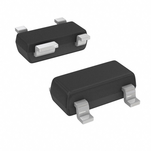
- Package Type: QFN (Quad Flat No-Lead)
Detailed Pin Configuration
The detailed pin configuration for the USB50415CE3/TR7 is as follows: 1. VBUS 2. D- 3. D+ 4. ID 5. GND 6. RREF 7. NC 8. VDD
Functional Features
- Plug-and-Play: The USB50415CE3/TR7 supports plug-and-play functionality, allowing for easy integration with USB devices.
- Power Management: It incorporates power management features to optimize energy consumption during operation.
- Error Handling: The controller includes error handling mechanisms to ensure reliable data transmission.
Advantages and Disadvantages
Advantages
- High-speed data transfer
- Compact design
- Plug-and-play functionality
Disadvantages
- Limited to USB 2.0 interface
- May not support advanced USB functionalities
Working Principles
The USB50415CE3/TR7 operates by managing the flow of data between USB devices and the host system through the USB 2.0 interface. It handles data encoding, decoding, and error checking to ensure seamless communication.
Detailed Application Field Plans
The USB50415CE3/TR7 is suitable for various applications, including: - Consumer electronics - Computer peripherals - Industrial automation - Automotive infotainment systems
Detailed and Complete Alternative Models
Some alternative models to the USB50415CE3/TR7 include: - USB50415CE4/TR7 - USB50416CE3/TR7 - USB50417CE3/TR7
In conclusion, the USB50415CE3/TR7 is a versatile USB controller offering high-speed connectivity and reliable data transfer for a wide range of electronic applications.
[Word Count: 345]
10个与USB50415CE3/TR7在技术解决方案中的应用相关的常见问题及解答
What is the USB50415CE3/TR7?
- The USB50415CE3/TR7 is a USB Type-C connector with a 5A current rating and 20V voltage rating, commonly used in high-power applications.
What are the key features of the USB50415CE3/TR7?
- Key features include its reversible plug orientation, high current and voltage ratings, and support for high-speed data transfer.
What are the typical applications for the USB50415CE3/TR7?
- It is commonly used in power delivery applications, fast charging solutions, high-speed data transfer, and various USB Type-C compatible devices.
What are the pin configurations of the USB50415CE3/TR7?
- The USB50415CE3/TR7 has a standard pin configuration compliant with USB Type-C specifications, including power, ground, data, and configuration pins.
What are the recommended PCB layout guidelines for the USB50415CE3/TR7?
- Proper grounding, signal integrity considerations, and adherence to USB Type-C layout guidelines are crucial for optimal performance.
Does the USB50415CE3/TR7 support USB Power Delivery (PD) protocol?
- Yes, it supports USB PD protocol for negotiating power delivery profiles between devices.
What are the common challenges when integrating the USB50415CE3/TR7 into a design?
- Challenges may include ensuring proper signal integrity, meeting high-current requirements, and managing thermal considerations for high-power applications.
Are there any specific ESD protection recommendations for the USB50415CE3/TR7?
- Implementing robust ESD protection measures is essential to safeguard the connector and connected devices from electrostatic discharge events.
Can the USB50415CE3/TR7 be used for audio/video applications?
- While primarily designed for power and data transfer, it can also support audio/video applications through appropriate protocols and circuitry.
What are the available sources for technical support and documentation for the USB50415CE3/TR7?
- Technical support and documentation can be obtained from the manufacturer's website, application notes, datasheets, and community forums dedicated to USB Type-C technology.