

74LVC2G34GV,125
Basic Information Overview
- Category: Integrated Circuit (IC)
- Use: Logic Gate
- Characteristics: Dual Buffer/Inverter with Open Drain Output
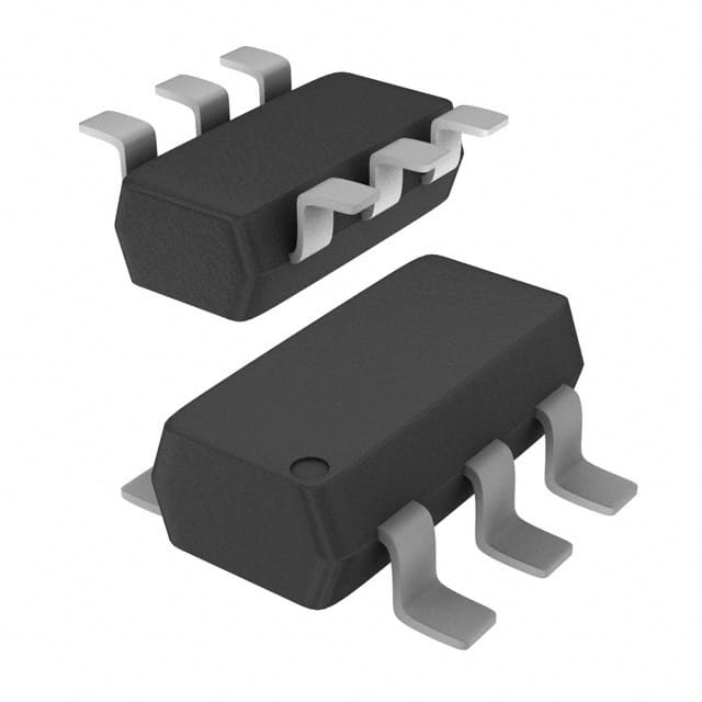
- Package: SOT753 (SC-70)
- Essence: High-speed CMOS technology
- Packaging/Quantity: Tape and Reel, 3000 pieces per reel
Specifications
- Supply Voltage Range: 1.65V to 5.5V
- High-Level Input Voltage: 0.7 x VCC
- Low-Level Input Voltage: 0.3 x VCC
- High-Level Output Voltage: VCC - 0.4V
- Low-Level Output Voltage: 0.4V
- Maximum Operating Frequency: 400 MHz
- Propagation Delay: 3.8 ns (typical)
Detailed Pin Configuration
The 74LVC2G34GV,125 has a total of 6 pins: 1. A: Input A 2. Y: Output Y 3. GND: Ground 4. B: Input B 5. Y: Output Y 6. VCC: Power Supply
Functional Features
- Dual buffer/inverter with open drain output
- Wide supply voltage range allows compatibility with various systems
- High-speed operation suitable for applications requiring fast signal processing
- Open drain output allows easy interfacing with other devices
- Low power consumption
Advantages
- Small package size enables space-saving designs
- Wide supply voltage range provides flexibility in different applications
- High-speed operation enhances overall system performance
- Open drain output facilitates communication between different logic levels
- Low power consumption helps prolong battery life in portable devices
Disadvantages
- Limited number of inputs and outputs restricts the complexity of circuits that can be implemented
- Open drain output requires external pull-up resistors for proper signal level translation
- Sensitivity to electrostatic discharge (ESD) requires careful handling during assembly and usage
Working Principles
The 74LVC2G34GV,125 is based on high-speed CMOS technology. It consists of two independent buffer/inverter circuits with open drain outputs. The inputs are compatible with both TTL and CMOS logic levels, allowing seamless integration into various systems. The open drain outputs provide a flexible interface for connecting to other devices, enabling bidirectional communication.
Detailed Application Field Plans
The 74LVC2G34GV,125 finds applications in a wide range of fields, including: 1. Communication Systems: Used for level shifting and signal buffering in data transmission circuits. 2. Industrial Automation: Employed in control systems for interfacing between different logic levels. 3. Consumer Electronics: Integrated into portable devices for voltage level conversion and signal amplification. 4. Automotive Electronics: Utilized in automotive control units for reliable signal processing and interfacing.
Detailed and Complete Alternative Models
Some alternative models that offer similar functionality to the 74LVC2G34GV,125 include: - SN74LVC2G34DBVR (Texas Instruments) - MC74VHC2G34DTT1G (ON Semiconductor) - TC7SZ34FU (Toshiba)
Note: These alternative models may have slight variations in specifications and package options.
10个与74LVC2G34GV,125在技术解决方案中的应用相关的常见问题及解答
Sure! Here are 10 common questions and answers related to the application of 74LVC2G34GV,125 in technical solutions:
Q: What is the function of the 74LVC2G34GV,125? A: The 74LVC2G34GV,125 is a dual buffer with Schmitt-trigger inputs. It is used to amplify and shape digital signals.
Q: What is the operating voltage range for the 74LVC2G34GV,125? A: The operating voltage range for this IC is typically between 1.65V and 5.5V.
Q: Can the 74LVC2G34GV,125 be used as a level shifter? A: Yes, it can be used as a level shifter to convert signals between different voltage levels.
Q: What is the maximum output current of the 74LVC2G34GV,125? A: The maximum output current is typically around 32mA.
Q: Does the 74LVC2G34GV,125 have internal pull-up or pull-down resistors? A: No, it does not have internal pull-up or pull-down resistors. External resistors may be required for certain applications.
Q: Can the 74LVC2G34GV,125 handle high-speed signals? A: Yes, it is designed to operate at high speeds and has a propagation delay of typically 4.3ns.
Q: Is the 74LVC2G34GV,125 compatible with both CMOS and TTL logic levels? A: Yes, it is compatible with both CMOS and TTL logic levels.
Q: How many inputs and outputs does the 74LVC2G34GV,125 have? A: It has two inputs and two outputs.
Q: Can the 74LVC2G34GV,125 be used in battery-powered applications? A: Yes, it can be used in battery-powered applications as it has a low power consumption.
Q: What is the package type of the 74LVC2G34GV,125? A: It is available in various package types, such as SOT23 and XSON.