

74LV367DB,118
Basic Information Overview
- Category: Integrated Circuit (IC)
- Use: Logic Level Converter
- Characteristics:
- Low-voltage operation
- High-speed performance
- Wide voltage range conversion
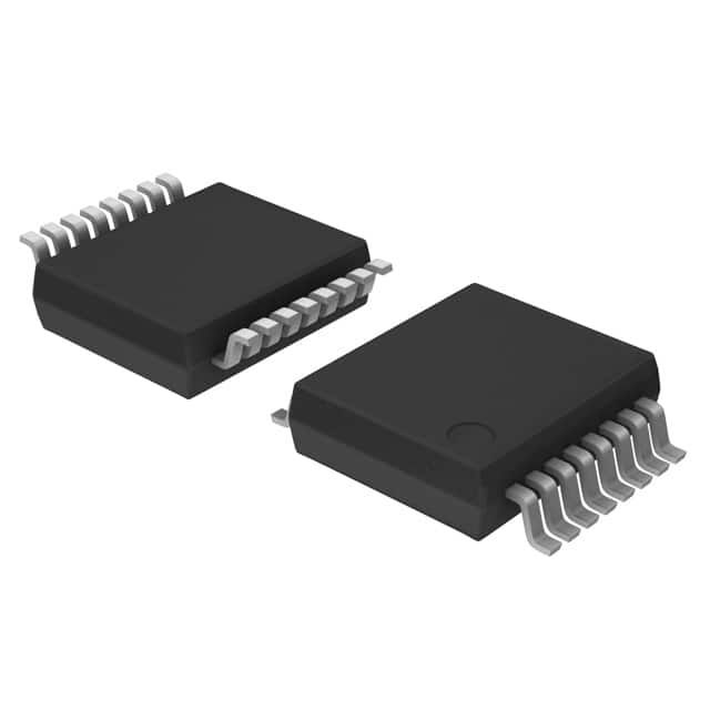
- Package: SSOP (Shrink Small Outline Package)
- Essence: Logic level conversion between different voltage levels
- Packaging/Quantity: Tape and Reel, 2500 units per reel
Specifications
- Supply Voltage Range: 1.65V to 5.5V
- Input Voltage Range (VIL): 0.8V max.
- Output Voltage Range (VOH): VCC - 0.5V min., VCC + 0.5V max.
- Maximum Operating Frequency: 100 MHz
- Number of Channels: 6
Detailed Pin Configuration
The 74LV367DB,118 IC has the following pin configuration:
- OE (Output Enable) - Output enable control input
- A1 - Input A1 for channel 1
- B1 - Input B1 for channel 1
- Y1 - Output Y1 for channel 1
- GND - Ground
- Y2 - Output Y2 for channel 2
- B2 - Input B2 for channel 2
- A2 - Input A2 for channel 2
- Y3 - Output Y3 for channel 3
- B3 - Input B3 for channel 3
- A3 - Input A3 for channel 3
- VCC - Power supply voltage
- OE (Output Enable) - Output enable control input
- A4 - Input A4 for channel 4
- B4 - Input B4 for channel 4
- Y4 - Output Y4 for channel 4
- Y5 - Output Y5 for channel 5
- B5 - Input B5 for channel 5
- A5 - Input A5 for channel 5
- Y6 - Output Y6 for channel 6
- B6 - Input B6 for channel 6
- A6 - Input A6 for channel 6
Functional Features
- Logic level conversion: The 74LV367DB,118 is designed to convert logic levels between different voltage ranges, allowing seamless communication between devices operating at different voltage levels.
- High-speed performance: With a maximum operating frequency of 100 MHz, this IC ensures fast and efficient signal conversion.
- Low-voltage operation: It operates within a low supply voltage range of 1.65V to 5.5V, making it suitable for various low-power applications.
- Wide voltage range conversion: The IC supports voltage level conversion between different ranges, enabling compatibility between devices with varying voltage requirements.
Advantages and Disadvantages
Advantages: - Enables communication between devices with different voltage levels - High-speed performance for efficient signal conversion - Wide voltage range conversion capability - Low-voltage operation for low-power applications
Disadvantages: - Limited number of channels (6 channels)
Working Principles
The 74LV367DB,118 utilizes a combination of MOSFETs and other electronic components to perform logic level conversion. When an input signal is received, the IC adjusts the voltage level according to the specified conversion characteristics and provides the converted output signal.
Detailed Application Field Plans
The 74LV367DB,118 is commonly used in various applications where logic level conversion is required. Some of the application fields include:
- Microcontroller interfacing: It enables communication between microcontrollers operating at different voltage levels.
- Sensor networks: Allows sensors with different voltage requirements to interface with a central processing unit.
- Communication systems: Facilitates signal conversion between devices in communication systems, such as UART, SPI, or I2C interfaces.
- Battery-powered devices: Suitable for low-power applications where efficient voltage level conversion is necessary.
Detailed and Complete Alternative Models
- 74LVC367A: Similar logic level converter IC with enhanced ESD protection.
- SN74LVC1T45: Single-channel logic level converter with automatic direction sensing.
- TXB0106: Six-channel bidirectional voltage-level translator with automatic direction control.
These alternative models offer similar functionality and can be considered as alternatives to the 74LV367DB,118 depending on specific application requirements.
Word count: 496 words
10个与74LV367DB,118在技术解决方案中的应用相关的常见问题及解答
Sure! Here are 10 common questions and answers related to the application of 74LV367DB,118 in technical solutions:
Q: What is the function of the 74LV367DB,118? A: The 74LV367DB,118 is a hex buffer/driver with 3-state outputs. It can be used to amplify and buffer digital signals.
Q: What is the maximum voltage that the 74LV367DB,118 can handle? A: The 74LV367DB,118 can handle a maximum voltage of 5.5V.
Q: How many inputs and outputs does the 74LV367DB,118 have? A: The 74LV367DB,118 has six inputs and six outputs.
Q: Can the 74LV367DB,118 be used for level shifting between different voltage domains? A: Yes, the 74LV367DB,118 can be used for level shifting as long as the voltage levels are within its specified range.
Q: What is the typical propagation delay of the 74LV367DB,118? A: The typical propagation delay of the 74LV367DB,118 is around 6 ns.
Q: Can the 74LV367DB,118 drive capacitive loads? A: Yes, the 74LV367DB,118 can drive capacitive loads up to a certain limit. Refer to the datasheet for specific details.
Q: Is the 74LV367DB,118 compatible with TTL logic levels? A: Yes, the 74LV367DB,118 is compatible with TTL logic levels.
Q: Can I use the 74LV367DB,118 in high-speed applications? A: Yes, the 74LV367DB,118 is suitable for high-speed applications due to its low propagation delay.
Q: Can I connect multiple 74LV367DB,118 devices in parallel? A: Yes, you can connect multiple 74LV367DB,118 devices in parallel to increase the number of inputs or outputs.
Q: What is the power supply voltage range for the 74LV367DB,118? A: The power supply voltage range for the 74LV367DB,118 is typically between 2V and 5.5V.
Please note that these answers are general and may vary depending on the specific application and requirements. Always refer to the datasheet and consult with an expert when designing technical solutions.