

产品详情请参阅规格.
PDTA114YK,115
Product Overview
- Category: Transistor
- Use: Amplification and switching of electronic signals
- Characteristics: Small signal NPN transistor, high current gain, low voltage drop
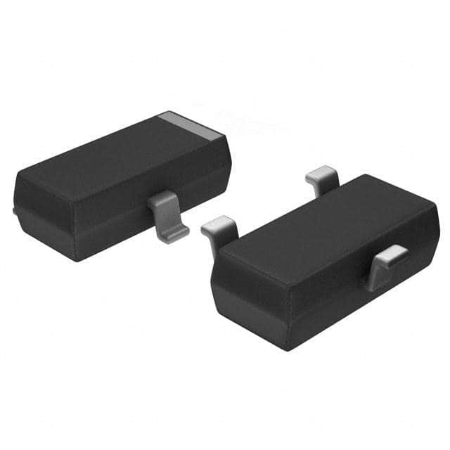
- Package: SOT416 (SC-75)
- Essence: High-performance small-signal transistor
- Packaging/Quantity: Tape and reel, 3000 units per reel
Specifications
- Type: NPN
- VCEO: 50V
- IC: 100mA
- hFE: 100 to 600
- Ptot: 200mW
- fT: 250MHz
Detailed Pin Configuration
- Base (B)
- Emitter (E)
- Collector (C)
Functional Features
- High current gain
- Low voltage drop
- Small package size
Advantages
- Suitable for high-density applications
- Fast switching speed
- Low power consumption
Disadvantages
- Limited power dissipation capability
- Sensitive to overvoltage conditions
Working Principles
The PDTA114YK,115 operates as a small-signal NPN transistor, amplifying and switching electronic signals. When a small current flows into the base (B) terminal, it controls a larger current flowing between the collector (C) and emitter (E) terminals.
Detailed Application Field Plans
- Audio amplification circuits
- Sensor interface circuits
- Signal conditioning circuits
Detailed and Complete Alternative Models
- BC847B,215
- MMBT3904,215
- 2N3904
This comprehensive entry provides an in-depth understanding of the PDTA114YK,115, covering its specifications, pin configuration, functional features, advantages, disadvantages, working principles, application field plans, and alternative models.
10个与PDTA114YK,115在技术解决方案中的应用相关的常见问题及解答
What is PDTA114YK,115?
- PDTA114YK,115 is a high-performance NPN resistor-equipped transistor in a small SOT883B Surface-Mounted Device (SMD) plastic package.
What are the typical applications of PDTA114YK,115?
- It is commonly used in general-purpose switching and amplification applications in technical solutions.
What is the maximum collector current for PDTA114YK,115?
- The maximum collector current for PDTA114YK,115 is 100 mA.
What is the voltage rating for PDTA114YK,115?
- The voltage rating for PDTA114YK,115 is 50 V.
What are the key features of PDTA114YK,115?
- Some key features include low collector-emitter saturation voltage, high current gain, and low power dissipation.
Can PDTA114YK,115 be used in high-frequency applications?
- Yes, PDTA114YK,115 can be used in high-frequency applications due to its high transition frequency.
Is PDTA114YK,115 suitable for use in portable electronic devices?
- Yes, PDTA114YK,115 is suitable for use in portable electronic devices due to its small SMD package and low power dissipation.
What are the recommended operating conditions for PDTA114YK,115?
- The recommended operating conditions include a collector current of 10 mA to 100 mA and an operating temperature range of -55°C to +150°C.
Does PDTA114YK,115 require external resistors for biasing?
- No, PDTA114YK,115 comes with built-in resistors, eliminating the need for external biasing resistors.
Are there any alternative components that can be used in place of PDTA114YK,115?
- Alternative components with similar specifications include PDTA114YE,115 and PDTA114ET,115.