

PMBFJ177,215
Product Overview
- Category: Semiconductor
- Use: Amplification and switching of low-power signals
- Characteristics: High gain, low noise, small package size
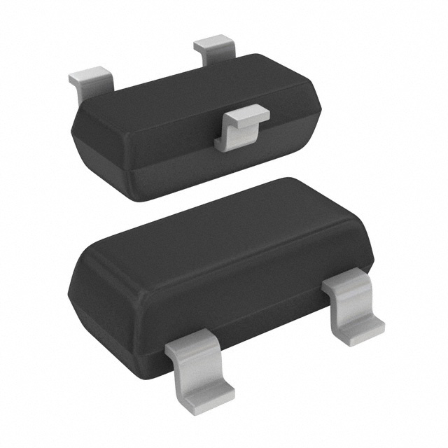
- Package: SOT23, SMD
- Essence: N-channel junction field-effect transistor (JFET)
- Packaging/Quantity: Tape and reel, 3000 units per reel
Specifications
- Maximum Drain-Source Voltage: 30 V
- Maximum Gate-Source Voltage: ±20 V
- Maximum Continuous Drain Current: 10 mA
- Power Dissipation: 225 mW
- Operating Temperature Range: -55°C to +150°C
Detailed Pin Configuration
- Pin 1 (Source)
- Pin 2 (Gate)
- Pin 3 (Drain)
Functional Features
- High input impedance
- Low output capacitance
- Low noise figure
Advantages
- Small package size
- High gain
- Low noise
Disadvantages
- Limited maximum drain-source voltage
- Limited maximum continuous drain current
Working Principles
The PMBFJ177,215 operates based on the field effect controlled by the voltage applied to the gate terminal. It allows for amplification and switching of low-power signals with high input impedance and low output capacitance.
Detailed Application Field Plans
- Audio amplification circuits
- Sensor signal amplification
- Low-frequency signal switching
Detailed and Complete Alternative Models
- J175
- J176
- J177
This semiconductor device, PMBFJ177,215, is widely used in various electronic applications due to its small package size, high gain, and low noise characteristics. Its limitations in terms of maximum voltage and current are important considerations when selecting alternative models for specific applications.
Word count: 248
10个与PMBFJ177,215在技术解决方案中的应用相关的常见问题及解答
What is PMBFJ177,215?
- PMBFJ177,215 is a field-effect transistor (FET) designed for low noise amplifier applications in the UHF frequency range.
What are the key features of PMBFJ177,215?
- The key features include low noise figure, high gain, and low power consumption, making it suitable for use in various technical solutions.
What is the typical application of PMBFJ177,215?
- PMBFJ177,215 is commonly used in radio frequency (RF) amplifiers, signal processing circuits, and communication systems where low noise performance is critical.
What are the electrical characteristics of PMBFJ177,215?
- The electrical characteristics include a low noise figure of typically 0.8 dB, a high gain of typically 15 dB, and a low input capacitance of typically 0.6 pF.
How does PMBFJ177,215 compare to other similar transistors?
- PMBFJ177,215 offers lower noise figure and higher gain compared to many other FETs in its class, making it a preferred choice for low noise applications.
What are the recommended operating conditions for PMBFJ177,215?
- The recommended operating voltage is typically around 5V, with a maximum drain-source voltage of 20V and a maximum continuous drain current of 10mA.
Can PMBFJ177,215 be used in high-frequency applications?
- Yes, PMBFJ177,215 is designed for operation in the UHF frequency range, making it suitable for high-frequency applications.
Are there any specific layout considerations when using PMBFJ177,215?
- It is important to minimize parasitic capacitances and inductances in the layout to ensure optimal performance of PMBFJ177,215 in technical solutions.
What are the potential challenges when integrating PMBFJ177,215 into a design?
- One potential challenge is ensuring proper matching and biasing to achieve the desired performance, especially in high-frequency and low-noise applications.
Where can I find detailed application notes and reference designs for PMBFJ177,215?
- Detailed application notes and reference designs for PMBFJ177,215 can be found on the manufacturer's website or in technical literature related to RF and microwave circuit design.