

FJN3309RBU Product Overview
Introduction
The FJN3309RBU is a semiconductor product belonging to the category of integrated circuits. This component is widely used in electronic devices for various applications due to its specific characteristics and functional features.
Basic Information Overview
- Category: Integrated Circuits
- Use: Electronic devices and circuitry
- Characteristics: High performance, low power consumption, compact size
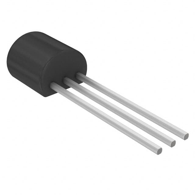
- Package: SOT-23-3
- Essence: Amplification and signal processing
- Packaging/Quantity: Typically packaged in reels of 3000 units
Specifications
- Type: NPN Transistor
- Maximum Collector-Emitter Voltage (Vce): 50V
- Maximum Collector Current (Ic): 100mA
- Maximum Power Dissipation (Pd): 225mW
- Operating Temperature Range: -55°C to 150°C
Detailed Pin Configuration
The FJN3309RBU has a standard SOT-23-3 package with the following pin configuration: 1. Base (B) 2. Emitter (E) 3. Collector (C)
Functional Features
- High gain and bandwidth
- Low noise and distortion
- Fast switching speed
- Small footprint and low profile
Advantages and Disadvantages
Advantages
- Compact size allows for integration into small form factor devices
- Low power consumption contributes to energy efficiency
- High performance characteristics enable reliable signal processing
Disadvantages
- Limited maximum collector current may restrict use in high-power applications
- Operating temperature range may not be suitable for extreme environments
Working Principles
The FJN3309RBU operates as an NPN transistor, amplifying and processing electrical signals based on the input at the base terminal. When a small current flows into the base, it controls a larger current flow between the collector and emitter, enabling signal amplification and switching functions.
Detailed Application Field Plans
The FJN3309RBU is commonly utilized in the following application fields: - Audio amplifiers - Signal processing circuits - Sensor interfaces - Low-power switching circuits
Detailed and Complete Alternative Models
- FJN3309R: Similar specifications and characteristics
- FJN3308RBU: Lower power dissipation, suitable for low-power applications
- FJN3310RBU: Higher maximum collector current, suitable for higher power applications
In conclusion, the FJN3309RBU is a versatile integrated circuit with specific characteristics and functional features that make it suitable for various electronic applications, especially those requiring low power consumption and compact size.
Word count: 410
10个与FJN3309RBU在技术解决方案中的应用相关的常见问题及解答
What is FJN3309RBU?
- FJN3309RBU is a high-power, low-loss N-channel MOSFET designed for use in various technical solutions requiring efficient power management.
What are the key features of FJN3309RBU?
- The key features of FJN3309RBU include a low on-resistance, high current capability, and a compact package design for easy integration into different applications.
What are the typical applications of FJN3309RBU?
- FJN3309RBU is commonly used in applications such as motor control, power supplies, DC-DC converters, and battery management systems.
What is the maximum voltage and current rating for FJN3309RBU?
- FJN3309RBU has a maximum voltage rating of [insert voltage] and a maximum current rating of [insert current].
What are the thermal characteristics of FJN3309RBU?
- The thermal resistance and junction temperature of FJN3309RBU are important considerations for designing heat dissipation solutions in high-power applications.
Does FJN3309RBU require any specific gate driver circuitry?
- Yes, FJN3309RBU may require specific gate driver circuitry to ensure optimal performance and reliability in different technical solutions.
Are there any recommended layout guidelines for using FJN3309RBU in PCB designs?
- Yes, following recommended layout guidelines can help minimize parasitic effects and optimize the performance of FJN3309RBU in PCB designs.
What are the environmental and compliance specifications for FJN3309RBU?
- FJN3309RBU complies with relevant environmental regulations and may have specific operating temperature ranges and certifications for different markets.
Can FJN3309RBU be used in automotive applications?
- Yes, FJN3309RBU may be suitable for certain automotive applications, but it's important to verify its compatibility with automotive standards and requirements.
Where can I find detailed technical documentation and application notes for FJN3309RBU?
- Detailed technical documentation and application notes for FJN3309RBU can typically be found on the manufacturer's website or through authorized distributors.