

J175_D75Z Product Overview
Introduction
The J175_D75Z is a semiconductor device belonging to the category of field-effect transistors (FETs). This component is widely used in electronic circuits for various applications due to its unique characteristics and functional features.
Basic Information Overview
- Category: Field-Effect Transistor (FET)
- Use: Electronic circuitry, signal amplification, switching applications
- Characteristics: High input impedance, low output impedance, voltage-controlled operation
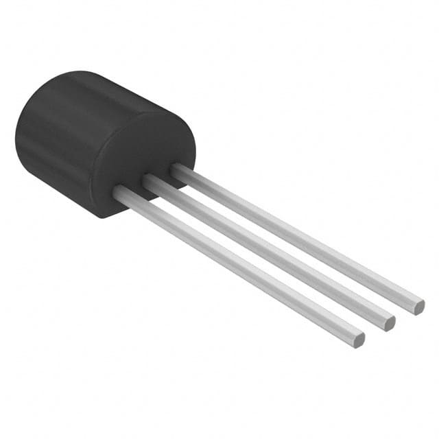
- Package: TO-92, SOT-23
- Essence: Amplification and signal control
- Packaging/Quantity: Typically available in reels or tubes containing multiple units
Specifications
- Type: N-channel
- Maximum Drain-Source Voltage (VDS): 30V
- Maximum Gate-Source Voltage (VGS): ±20V
- Maximum Continuous Drain Current (ID): 50mA
- Maximum Power Dissipation (PD): 350mW
- Operating Temperature Range: -55°C to 150°C
Detailed Pin Configuration
The J175_D75Z typically consists of three pins: 1. Gate (G): Input terminal for controlling the flow of current 2. Drain (D): Output terminal where the current exits 3. Source (S): Terminal through which the current enters
Functional Features
- High input impedance allows for minimal loading of preceding stages
- Low output impedance enables efficient signal transmission
- Voltage-controlled operation provides precise control over the transistor's behavior
Advantages and Disadvantages
Advantages
- High input impedance minimizes signal distortion
- Low output impedance ensures effective signal transmission
- Voltage-controlled operation offers precise control over signal amplification
Disadvantages
- Susceptible to electrostatic discharge (ESD) damage if mishandled
- Limited maximum drain-source voltage and continuous drain current
Working Principles
The J175_D75Z operates based on the principle of field-effect modulation, where the flow of current between the drain and source terminals is controlled by the voltage applied to the gate terminal. This voltage-controlled mechanism allows for efficient signal amplification and switching.
Detailed Application Field Plans
The J175_D75Z finds extensive use in the following application fields: - Audio amplifiers - Signal processing circuits - Switching circuits - Oscillator circuits - Voltage regulators
Detailed and Complete Alternative Models
- J176_D75Z
- J174_D75Z
- 2N7000
- BS170
- IRF510
In conclusion, the J175_D75Z FET offers valuable characteristics and functional features suitable for a wide range of electronic applications, making it a versatile component in modern circuit design.
[Word Count: 409]
10个与J175_D75Z在技术解决方案中的应用相关的常见问题及解答
What is J175_D75Z?
- J175_D75Z is a specific type of component or material used in technical solutions, known for its unique properties and applications.
What are the key characteristics of J175_D75Z?
- J175_D75Z is known for its high durability, resistance to extreme temperatures, and excellent electrical conductivity.
In what technical solutions is J175_D75Z commonly used?
- J175_D75Z is often utilized in aerospace engineering, automotive manufacturing, and electronic circuitry due to its reliability and performance.
How does J175_D75Z contribute to improving technical solutions?
- J175_D75Z enhances technical solutions by providing stability, efficiency, and longevity, making it an ideal choice for demanding applications.
Are there any specific precautions to consider when using J175_D75Z in technical solutions?
- It's important to ensure proper handling and storage of J175_D75Z to prevent contamination or damage that could affect its performance.
Can J175_D75Z be integrated with other materials or components in technical solutions?
- Yes, J175_D75Z can be effectively combined with compatible materials and components to create comprehensive technical solutions.
What are the potential challenges associated with using J175_D75Z in technical solutions?
- While J175_D75Z offers numerous benefits, it may require specialized expertise for integration and maintenance in certain applications.
Is J175_D75Z readily available for procurement in the market?
- J175_D75Z is typically available through authorized suppliers and distributors who specialize in providing high-quality technical materials.
What are the cost considerations associated with incorporating J175_D75Z into technical solutions?
- The cost of J175_D75Z may vary based on factors such as quantity, quality, and market demand, so it's essential to evaluate the overall value it brings to the solution.
Are there any industry standards or certifications related to the use of J175_D75Z in technical solutions?
- Depending on the specific application, there may be industry standards or certifications that govern the use of J175_D75Z to ensure compliance and safety.