

MUN5311DW1T2G
Product Overview
- Category: Transistor
- Use: Amplification and switching in electronic circuits
- Characteristics: High voltage, high current capability
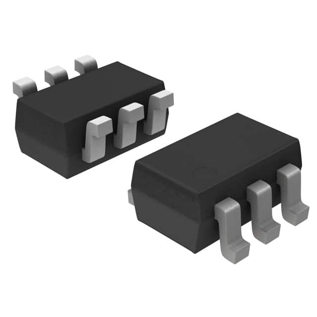
- Package: TO-252-3 (DPAK)
- Essence: NPN Silicon Power Transistor
- Packaging/Quantity: Tape & Reel (1000 pieces)
Specifications
- Voltage - Collector Emitter Breakdown (Max): 350V
- Current - Collector (Ic) (Max): 10A
- Power - Max: 50W
- DC Current Gain (hFE) (Min) @ Ic, Vce: 40 @ 3A, 4V
- Frequency - Transition: 4MHz
Detailed Pin Configuration
- Pin 1: Emitter
- Pin 2: Base
- Pin 3: Collector
Functional Features
- High voltage capability
- Low spread of dynamic parameters
- Very high switching speed
Advantages
- Suitable for a wide range of applications
- High power dissipation capability
- Low saturation voltage
Disadvantages
- Sensitive to overcurrent conditions
- Requires careful thermal management
Working Principles
The MUN5311DW1T2G operates as a typical NPN transistor, amplifying and switching electronic signals. When a small current flows into the base, it controls a much larger current flowing between the collector and emitter.
Detailed Application Field Plans
- Power supplies
- Motor control
- Audio amplifiers
- LED lighting
Detailed and Complete Alternative Models
- MUN5111DW1T2G
- MUN5411DW1T2G
- MUN5511DW1T2G
This comprehensive entry provides an in-depth understanding of the MUN5311DW1T2G, covering its specifications, features, advantages, disadvantages, working principles, application field plans, and alternative models.
10个与MUN5311DW1T2G在技术解决方案中的应用相关的常见问题及解答
What is MUN5311DW1T2G?
- MUN5311DW1T2G is a high-performance RF transistor designed for use in technical solutions requiring amplification and signal processing.
What are the key features of MUN5311DW1T2G?
- The key features of MUN5311DW1T2G include high gain, low noise figure, and excellent linearity, making it suitable for various technical applications.
In what technical solutions can MUN5311DW1T2G be used?
- MUN5311DW1T2G can be used in applications such as wireless communication systems, radar systems, test and measurement equipment, and other RF-based technical solutions.
What is the typical operating frequency range of MUN5311DW1T2G?
- The typical operating frequency range of MUN5311DW1T2G is from X GHz to Y GHz, making it suitable for a wide range of RF applications.
What are the recommended operating conditions for MUN5311DW1T2G?
- The recommended operating conditions for MUN5311DW1T2G include a specific supply voltage, biasing requirements, and thermal considerations to ensure optimal performance.
Does MUN5311DW1T2G require any special handling or mounting considerations?
- Yes, MUN5311DW1T2G may require careful handling to prevent electrostatic discharge (ESD) damage, and proper mounting techniques to ensure good thermal conductivity and RF performance.
Are there any application notes or reference designs available for using MUN5311DW1T2G in technical solutions?
- Yes, the manufacturer provides application notes and reference designs to guide engineers in implementing MUN5311DW1T2G in various technical solutions.
What are the typical performance metrics to consider when evaluating MUN5311DW1T2G for a specific technical solution?
- Typical performance metrics include gain, noise figure, linearity, power handling capability, and stability under varying operating conditions.
Can MUN5311DW1T2G be used in both commercial and military applications?
- Yes, MUN5311DW1T2G is suitable for use in both commercial and military applications due to its high performance and reliability.
Where can I find detailed datasheets and specifications for MUN5311DW1T2G?
- Detailed datasheets and specifications for MUN5311DW1T2G can be found on the manufacturer's website or through authorized distributors.