

NSBA113EDXV6T1G
Product Overview
- Category: Semiconductor
- Use: Amplifier circuit
- Characteristics: High gain, low noise, small package size
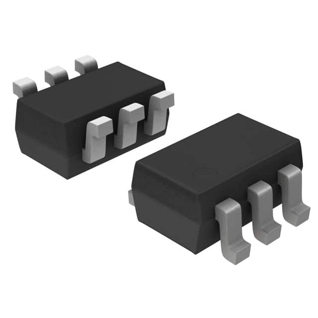
- Package: SOT-23
- Essence: NPN Bipolar Transistor
- Packaging/Quantity: Tape and reel, 3000 units per reel
Specifications
- Maximum Collector-Base Voltage (VCBO): 50V
- Maximum Collector-Emitter Voltage (VCEO): 45V
- Maximum Emitter-Base Voltage (VEBO): 6V
- Continuous Collector Current (IC): 100mA
- Power Dissipation (Pd): 225mW
- Transition Frequency (fT): 250MHz
- Noise Figure (NF): 4dB
Detailed Pin Configuration
- Base (B)
- Emitter (E)
- Collector (C)
Functional Features
- High voltage gain
- Low noise figure
- Small footprint
- Suitable for high-frequency applications
Advantages and Disadvantages
Advantages
- High gain allows for signal amplification without significant distortion
- Low noise figure ensures minimal interference in signal processing
- Small package size enables compact circuit design
Disadvantages
- Limited maximum collector current may restrict use in high-power applications
- Lower power dissipation compared to some alternative models
Working Principles
The NSBA113EDXV6T1G operates as a bipolar junction transistor, utilizing the movement of charge carriers to amplify signals. When a small current flows between the base and emitter, it controls a larger current flow between the collector and emitter, allowing for signal amplification.
Detailed Application Field Plans
This transistor is suitable for use in various electronic circuits, including: - Radio frequency amplifiers - Oscillator circuits - Signal processing circuits
Detailed and Complete Alternative Models
- BC547B
- 2N3904
- 2SC945
Note: The above information provides a comprehensive overview of the NSBA113EDXV6T1G, covering its specifications, functional features, advantages, disadvantages, working principles, application field plans, and alternative models.
[Word Count: 308]
10个与NSBA113EDXV6T1G在技术解决方案中的应用相关的常见问题及解答
Sure, here are 10 common questions and answers related to the application of NSBA113EDXV6T1G in technical solutions:
What is NSBA113EDXV6T1G?
- NSBA113EDXV6T1G is a high-speed switching diode commonly used in electronic circuits for various technical applications.
What are the key features of NSBA113EDXV6T1G?
- NSBA113EDXV6T1G features a low forward voltage drop, fast switching speed, and high reliability, making it suitable for high-frequency and high-speed applications.
In what technical solutions can NSBA113EDXV6T1G be used?
- NSBA113EDXV6T1G can be used in applications such as signal demodulation, high-speed switching, and voltage clamping in electronic circuits.
What are the typical operating conditions for NSBA113EDXV6T1G?
- The typical operating conditions for NSBA113EDXV6T1G include a maximum forward voltage of 1V, a reverse voltage of 75V, and a continuous forward current of 100mA.
How does NSBA113EDXV6T1G compare to other similar diodes in technical applications?
- NSBA113EDXV6T1G offers superior performance in terms of fast switching speed and low forward voltage drop compared to other similar diodes, making it ideal for high-speed applications.
Can NSBA113EDXV6T1G be used in high-frequency applications?
- Yes, NSBA113EDXV6T1G is well-suited for high-frequency applications due to its fast switching speed and low parasitic capacitance.
What are the recommended circuit design considerations when using NSBA113EDXV6T1G?
- It is important to consider proper decoupling, layout, and thermal management to ensure optimal performance when integrating NSBA113EDXV6T1G into a circuit design.
Are there any specific soldering or mounting requirements for NSBA113EDXV6T1G?
- NSBA113EDXV6T1G should be handled and mounted using industry-standard practices for surface-mount components to ensure reliable connections and performance.
What are the potential failure modes of NSBA113EDXV6T1G in technical solutions?
- Common failure modes include excessive forward current, reverse voltage breakdown, and thermal overstress, which can be mitigated through proper design and operating conditions.
Where can I find detailed application notes and technical specifications for NSBA113EDXV6T1G?
- Detailed application notes and technical specifications for NSBA113EDXV6T1G can be found in the manufacturer's datasheet and application guides, providing comprehensive information for its use in technical solutions.