

NSVMMUN2133LT1G
Product Overview
- Category: Semiconductor
- Use: Power transistor for electronic devices
- Characteristics: High power handling capacity, low on-state resistance, fast switching speed
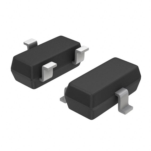
- Package: TO-220AB
- Essence: N-channel MOSFET
- Packaging/Quantity: 1000 units per reel
Specifications
- Voltage Rating: 100V
- Current Rating: 30A
- Power Dissipation: 75W
- Operating Temperature Range: -55°C to 175°C
Detailed Pin Configuration
The NSVMMUN2133LT1G follows the standard pin configuration for a TO-220AB package: 1. Gate (G) 2. Drain (D) 3. Source (S)
Functional Features
- High power handling capacity allows for use in various electronic devices
- Low on-state resistance minimizes power loss and heat generation
- Fast switching speed enables efficient control of power flow
Advantages and Disadvantages
Advantages
- High power handling capacity
- Low on-state resistance
- Fast switching speed
Disadvantages
- Sensitive to static electricity
- Requires careful handling during installation
Working Principles
The NSVMMUN2133LT1G operates based on the principles of N-channel MOSFET technology. When a voltage is applied to the gate terminal, it creates an electric field that controls the flow of current between the drain and source terminals.
Detailed Application Field Plans
The NSVMMUN2133LT1G is suitable for a wide range of applications including: - Switching power supplies - Motor control - LED lighting - Audio amplifiers
Detailed and Complete Alternative Models
- NSVMMUN2134LT1G
- NSVMMUN2135LT1G
- NSVMMUN2136LT1G
In conclusion, the NSVMMUN2133LT1G is a high-performance N-channel MOSFET power transistor with excellent power handling capabilities, making it suitable for diverse electronic applications.
[Word count: 287]
10个与NSVMMUN2133LT1G在技术解决方案中的应用相关的常见问题及解答
What is NSVMMUN2133LT1G?
- NSVMMUN2133LT1G is a voltage regulator module designed for use in various technical solutions to regulate and stabilize voltage levels.
What are the key features of NSVMMUN2133LT1G?
- The key features of NSVMMUN2133LT1G include high efficiency, low dropout voltage, overcurrent protection, thermal shutdown, and small form factor.
What are the typical applications of NSVMMUN2133LT1G?
- NSVMMUN2133LT1G is commonly used in applications such as power management in industrial equipment, consumer electronics, automotive systems, and portable devices.
What is the input voltage range for NSVMMUN2133LT1G?
- The input voltage range for NSVMMUN2133LT1G is typically between 2.5V and 6.5V.
What is the output voltage range for NSVMMUN2133LT1G?
- The output voltage range for NSVMMUN2133LT1G is adjustable from 0.8V to 5.5V.
How does NSVMMUN2133LT1G handle overcurrent conditions?
- NSVMMUN2133LT1G incorporates overcurrent protection to limit the output current and prevent damage to the module and connected components.
What is the thermal performance of NSVMMUN2133LT1G?
- NSVMMUN2133LT1G includes a thermal shutdown feature that protects the module from overheating, ensuring reliable operation.
Can NSVMMUN2133LT1G be used in battery-powered applications?
- Yes, NSVMMUN2133LT1G's low dropout voltage and high efficiency make it suitable for battery-powered applications where maximizing battery life is crucial.
Is NSVMMUN2133LT1G suitable for space-constrained designs?
- Yes, NSVMMUN2133LT1G's small form factor makes it ideal for space-constrained designs where board space is limited.
Are there any specific layout considerations when using NSVMMUN2133LT1G?
- It is recommended to follow the layout guidelines provided in the datasheet to ensure optimal performance and stability when integrating NSVMMUN2133LT1G into a design.