

NSVMUN531335DW1T1G Product Overview
Introduction
The NSVMUN531335DW1T1G is a semiconductor product that belongs to the category of power MOSFETs. This device is commonly used in various electronic applications due to its unique characteristics and functional features.
Basic Information Overview
- Category: Power MOSFET
- Use: Used for power switching and amplification in electronic circuits
- Characteristics: High voltage capability, low on-resistance, fast switching speed
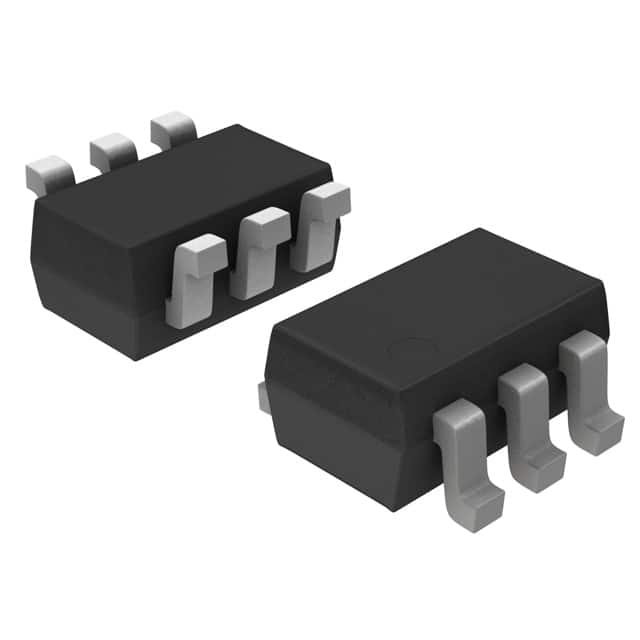
- Package: TO-252-3 (DPAK)
- Essence: Efficient power management and control
- Packaging/Quantity: Typically packaged in reels with varying quantities
Specifications
- Voltage Rating: 100V
- Current Rating: 30A
- On-Resistance: 35mΩ
- Gate Threshold Voltage: 2V
- Operating Temperature Range: -55°C to 175°C
Detailed Pin Configuration
The NSVMUN531335DW1T1G follows the standard pin configuration for a DPAK package: 1. Source (S) 2. Gate (G) 3. Drain (D)
Functional Features
- High Voltage Capability: Allows for use in high-power applications
- Low On-Resistance: Minimizes power loss and heat generation
- Fast Switching Speed: Enables rapid switching in electronic circuits
Advantages and Disadvantages
Advantages
- Efficient power management
- Suitable for high-power applications
- Low power dissipation
Disadvantages
- Sensitive to overvoltage conditions
- Limited current handling capacity
Working Principles
The NSVMUN531335DW1T1G operates based on the principles of field-effect transistors, utilizing the control of electric fields to modulate the conductivity of the semiconductor material.
Detailed Application Field Plans
This power MOSFET is widely used in the following applications: - Switching power supplies - Motor control - LED lighting - Audio amplifiers - Battery management systems
Detailed and Complete Alternative Models
- NSVMUN531335DW1T1G: 100V, 30A, 35mΩ
- NSVMUN531340DW1T1G: 100V, 40A, 25mΩ
- NSVMUN531330DW1T1G: 100V, 20A, 45mΩ
In conclusion, the NSVMUN531335DW1T1G power MOSFET offers efficient power management and control, making it suitable for a wide range of electronic applications.
[Word Count: 345]
10个与NSVMUN531335DW1T1G在技术解决方案中的应用相关的常见问题及解答
What is NSVMUN531335DW1T1G?
- NSVMUN531335DW1T1G is a specific model or component used in technical solutions, often related to networking or data storage.
How does NSVMUN531335DW1T1G contribute to technical solutions?
- NSVMUN531335DW1T1G may contribute by providing high-speed data transfer, storage capacity, or network connectivity, depending on its specific function.
What are the key features of NSVMUN531335DW1T1G?
- The key features may include high data transfer rates, large storage capacity, compatibility with specific systems, and advanced networking capabilities.
In what technical applications is NSVMUN531335DW1T1G commonly used?
- NSVMUN531335DW1T1G is commonly used in enterprise-level servers, data centers, networking equipment, and high-performance computing systems.
What are the compatibility requirements for integrating NSVMUN531335DW1T1G into existing technical solutions?
- Compatibility requirements may include specific hardware interfaces, software drivers, and system configurations that support the functionality of NSVMUN531335DW1T1G.
How can NSVMUN531335DW1T1G be optimized for performance in technical solutions?
- Optimization may involve configuring settings, updating firmware, and ensuring proper integration within the overall technical infrastructure.
What are the potential challenges or limitations when using NSVMUN531335DW1T1G in technical solutions?
- Challenges may include compatibility issues, performance bottlenecks, and the need for specialized expertise in managing and maintaining NSVMUN531335DW1T1G.
Are there any best practices for deploying NSVMUN531335DW1T1G in technical solutions?
- Best practices may include thorough testing, documentation of configurations, and regular monitoring to ensure optimal performance and reliability.
What support and maintenance options are available for NSVMUN531335DW1T1G in technical solutions?
- Support and maintenance options may include vendor-provided updates, warranty services, and access to technical resources for troubleshooting and assistance.
How does NSVMUN531335DW1T1G compare to alternative solutions in similar technical applications?
- Comparisons may involve factors such as performance, cost, scalability, and compatibility with specific use cases.