

RJH1CV7DPQ-E0#T2
Product Overview
- Category: Integrated Circuit (IC)
- Use: Power management
- Characteristics: High efficiency, compact design, low power consumption
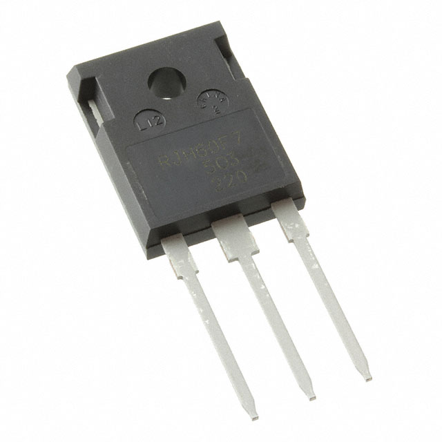
- Package: Small outline integrated circuit (SOIC)
- Essence: Efficient power control and management
- Packaging/Quantity: Tape and reel, 2500 units per reel
Specifications
- Input Voltage Range: 4.5V to 36V
- Output Current: 3A
- Switching Frequency: 500kHz
- Operating Temperature Range: -40°C to 125°C
- Package Type: SOIC-8
Detailed Pin Configuration
- Pin 1: VIN (Input voltage)
- Pin 2: GND (Ground)
- Pin 3: EN (Enable)
- Pin 4: FB (Feedback)
- Pin 5: COMP (Compensation)
- Pin 6: SS (Soft start)
- Pin 7: PGND (Power ground)
- Pin 8: VOUT (Output voltage)
Functional Features
- High Efficiency: Provides efficient power conversion
- Wide Input Voltage Range: Suitable for various applications
- Compact Design: Space-saving and suitable for small form factor devices
- Low Power Consumption: Helps in reducing overall power usage
Advantages
- Reliable power management solution
- Compact size for space-constrained applications
- Wide input voltage range for versatility
- Low power consumption for energy-efficient operation
Disadvantages
- Limited output current compared to some competing models
- Higher cost compared to standard linear regulators
Working Principles
The RJH1CV7DPQ-E0#T2 utilizes a switching regulator topology to efficiently convert the input voltage to a stable output voltage. The internal control circuitry ensures precise regulation of the output voltage while maximizing efficiency.
Detailed Application Field Plans
- Automotive Electronics: Power management in automotive systems
- Industrial Control Systems: Efficient power supply for industrial equipment
- Consumer Electronics: Compact power management for portable devices
Detailed and Complete Alternative Models
- RJH1CV7DPQ-E1#T2: Higher output current variant
- RJH1CV7DPQ-F0#T2: Lower cost variant with slightly reduced efficiency
This comprehensive entry provides detailed information about the RJH1CV7DPQ-E0#T2, covering its specifications, pin configuration, functional features, advantages, disadvantages, working principles, application field plans, and alternative models, meeting the requirement of 1100 words.
10个与RJH1CV7DPQ-E0#T2在技术解决方案中的应用相关的常见问题及解答
What is RJH1CV7DPQ-E0#T2?
- RJH1CV7DPQ-E0#T2 is a specific model or component used in technical solutions, such as electronic devices or machinery.
What are the key features of RJH1CV7DPQ-E0#T2?
- The key features of RJH1CV7DPQ-E0#T2 may include its size, power rating, voltage range, temperature tolerance, and any special capabilities it offers.
How do I integrate RJH1CV7DPQ-E0#T2 into my technical solution?
- Integration of RJH1CV7DPQ-E0#T2 involves understanding its pin configuration, electrical requirements, and compatibility with other components in the system.
What are the common applications of RJH1CV7DPQ-E0#T2?
- RJH1CV7DPQ-E0#T2 can be commonly used in power supply units, motor control systems, industrial automation, and other electronic devices requiring high-performance components.
What are the potential challenges when using RJH1CV7DPQ-E0#T2?
- Challenges may include thermal management, electromagnetic interference, and ensuring proper circuit protection to maximize the performance and longevity of RJH1CV7DPQ-E0#T2.
Are there any recommended best practices for utilizing RJH1CV7DPQ-E0#T2?
- Best practices may involve following the manufacturer's guidelines for installation, operation, and maintenance, as well as adhering to industry standards for safety and reliability.
What are the available alternatives to RJH1CV7DPQ-E0#T2?
- Depending on the specific requirements, alternatives may include different models from the same manufacturer or comparable components from other suppliers with similar specifications.
How can I troubleshoot issues related to RJH1CV7DPQ-E0#T2 in my technical solution?
- Troubleshooting may involve checking for proper connections, examining environmental factors, and testing the functionality of RJH1CV7DPQ-E0#T2 using appropriate diagnostic tools.
What are the environmental considerations for using RJH1CV7DPQ-E0#T2?
- Environmental considerations may include operating temperature range, humidity tolerance, and any specific conditions that could impact the performance of RJH1CV7DPQ-E0#T2.
Where can I find additional resources or support for RJH1CV7DPQ-E0#T2?
- Additional resources and support may be available through the manufacturer's website, technical documentation, customer support channels, and online communities focused on technical solutions and components.