

STD70N03L
Product Overview
- Category: Power MOSFET
- Use: Switching applications in power supplies, motor control, and other high-current circuits
- Characteristics: Low on-resistance, high current capability, low gate charge
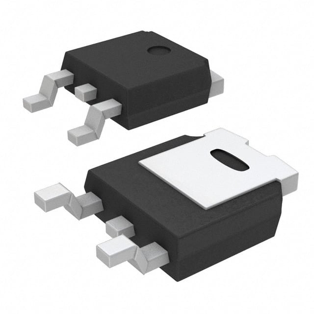
- Package: TO-252 (DPAK)
- Essence: Efficient power switching for various electronic applications
- Packaging/Quantity: Tape and reel, 2500 units per reel
Specifications
- Voltage Rating: 30V
- Current Rating: 70A
- On-Resistance: 8.5mΩ
- Gate Charge: 18nC
- Operating Temperature Range: -55°C to 175°C
Detailed Pin Configuration
The STD70N03L follows the standard pin configuration for a TO-252 package: 1. Source (S) 2. Gate (G) 3. Drain (D)
Functional Features
- Low on-resistance for minimal power dissipation
- High current capability for handling heavy loads
- Fast switching speed for efficient operation
- Low gate charge for reduced drive requirements
Advantages and Disadvantages
Advantages
- High current handling capacity
- Low on-resistance for minimal power loss
- Fast switching speed for improved efficiency
Disadvantages
- Sensitive to static discharge
- Limited voltage rating compared to some alternatives
Working Principles
The STD70N03L operates based on the principles of field-effect transistors, utilizing the control of the gate voltage to modulate the flow of current between the source and drain terminals.
Detailed Application Field Plans
The STD70N03L is suitable for a wide range of applications including: - Power supplies - Motor control systems - DC-DC converters - Battery management systems - Inverter circuits
Detailed and Complete Alternative Models
Some alternative models to consider include: - IRF3709ZPbF - FDP8870 - AOD4184
In conclusion, the STD70N03L Power MOSFET offers high current capability and low on-resistance, making it an ideal choice for various switching applications in electronic circuits.
Word Count: 297
10个与STD70N03L在技术解决方案中的应用相关的常见问题及解答
What is the maximum drain-source voltage of STD70N03L?
- The maximum drain-source voltage of STD70N03L is 30V.
What is the continuous drain current rating of STD70N03L?
- The continuous drain current rating of STD70N03L is 70A.
What is the on-state resistance (RDS(on)) of STD70N03L?
- The on-state resistance (RDS(on)) of STD70N03L is typically 0.004 ohms.
What are the typical applications for STD70N03L?
- STD70N03L is commonly used in power management, motor control, and other high-current switching applications.
Is STD70N03L suitable for automotive applications?
- Yes, STD70N03L is designed to meet the requirements for automotive applications.
What is the operating temperature range of STD70N03L?
- STD70N03L can operate within a temperature range of -55°C to 175°C.
Does STD70N03L have built-in protection features?
- STD70N03L includes built-in protection against overcurrent and thermal issues.
Can STD70N03L be used in parallel to handle higher currents?
- Yes, STD70N03L can be used in parallel to increase the current-handling capability.
What type of package does STD70N03L come in?
- STD70N03L is available in a TO-252 (DPAK) package.
Are there any recommended application circuits for STD70N03L?
- Yes, the datasheet for STD70N03L provides recommended application circuits for various technical solutions.