

STD80N10F7
Product Overview
- Category: Power MOSFET
- Use: Power switching applications
- Characteristics: High voltage, low on-resistance, fast switching speed
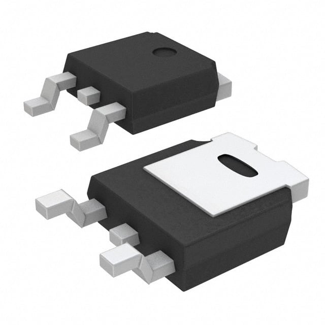
- Package: TO-252 (DPAK)
- Essence: Efficient power management
- Packaging/Quantity: Tape and reel, 2500 units per reel
Specifications
- Voltage Rating: 100V
- Current Rating: 80A
- On-Resistance: 10mΩ
- Gate Threshold Voltage: 2-4V
- Operating Temperature Range: -55°C to 175°C
Detailed Pin Configuration
The STD80N10F7 features a standard TO-252 (DPAK) package with three pins: 1. Gate (G): Input for controlling the switching operation 2. Drain (D): Connects to the load and the power supply 3. Source (S): Connected to the ground reference
Functional Features
- Fast switching speed for improved efficiency
- Low on-resistance for reduced power dissipation
- High voltage rating for versatile applications
Advantages and Disadvantages
Advantages
- High voltage rating allows for diverse application scenarios
- Low on-resistance enhances energy efficiency
- Fast switching speed improves overall performance
Disadvantages
- Sensitive to static electricity and voltage spikes
- Requires careful handling during installation and operation
Working Principles
The STD80N10F7 operates based on the principle of field-effect transistors, utilizing the gate voltage to control the flow of current between the drain and source terminals. When the gate voltage is applied, the MOSFET switches on, allowing current to pass through.
Detailed Application Field Plans
The STD80N10F7 is suitable for various power switching applications, including: - Motor control systems - Power supplies - Inverters - DC-DC converters - Battery management systems
Detailed and Complete Alternative Models
- STD90N10F7: Similar specifications with higher current rating
- STD70N10F7: Lower current rating with similar characteristics
- STD80P10F7: Complementary P-channel MOSFET for bidirectional switching applications
In conclusion, the STD80N10F7 Power MOSFET offers high voltage capability, low on-resistance, and fast switching speed, making it an ideal choice for various power management applications. Its robust design and efficient performance make it a valuable component in modern electronic systems.
Word count: 314
10个与STD80N10F7在技术解决方案中的应用相关的常见问题及解答
What is the maximum drain-source voltage of STD80N10F7?
- The maximum drain-source voltage of STD80N10F7 is 100V.
What is the continuous drain current rating of STD80N10F7?
- The continuous drain current rating of STD80N10F7 is 80A.
What is the on-resistance of STD80N10F7?
- The on-resistance of STD80N10F7 is typically 0.007 ohms.
Can STD80N10F7 be used in automotive applications?
- Yes, STD80N10F7 is suitable for automotive applications.
What is the operating temperature range of STD80N10F7?
- The operating temperature range of STD80N10F7 is -55°C to 175°C.
Is STD80N10F7 RoHS compliant?
- Yes, STD80N10F7 is RoHS compliant.
What type of package does STD80N10F7 come in?
- STD80N10F7 comes in a TO-252 (DPAK) package.
Does STD80N10F7 have built-in protection features?
- STD80N10F7 does not have built-in protection features and may require external circuitry for protection.
What are the typical applications of STD80N10F7?
- STD80N10F7 is commonly used in power management, motor control, and other high-current switching applications.
What is the gate threshold voltage of STD80N10F7?
- The gate threshold voltage of STD80N10F7 is typically 2.5V to 4V.