

Encyclopedia Entry: 74FCT2543CTSOCTG4
Product Overview
Category
The 74FCT2543CTSOCTG4 belongs to the category of integrated circuits (ICs).
Use
This IC is commonly used in electronic devices for signal switching and routing applications.
Characteristics
- High-speed operation
- Low power consumption
- Wide operating voltage range
- Compatibility with various logic families
- Robust design for reliable performance
Package
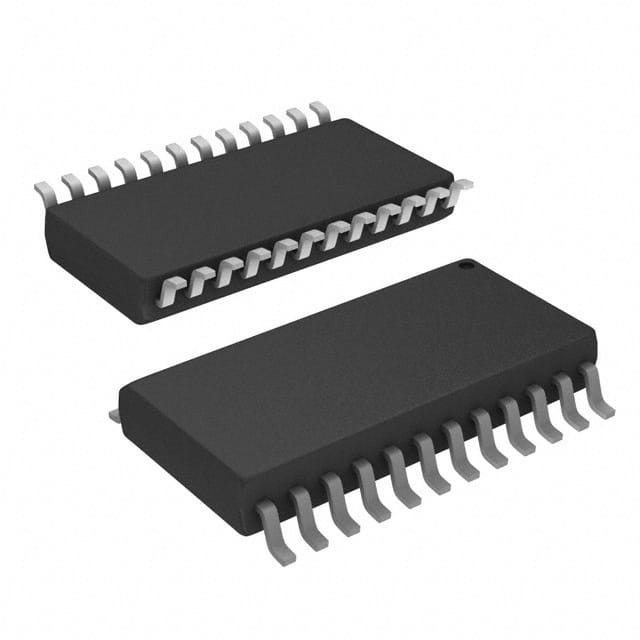
The 74FCT2543CTSOCTG4 is available in a small outline package (SO) with gull wing leads. This package offers ease of handling and compatibility with automated assembly processes.
Essence
The essence of the 74FCT2543CTSOCTG4 lies in its ability to efficiently switch and route signals within electronic circuits, enabling seamless communication between different components.
Packaging/Quantity
The IC is typically packaged in reels or tubes, containing a specific quantity per package. The exact packaging and quantity may vary depending on the manufacturer and supplier.
Specifications
- Supply Voltage: 2.0V to 5.5V
- Operating Temperature Range: -40°C to +85°C
- Input/Output Logic Levels: TTL/CMOS compatible
- Number of Channels: 8
- Switching Speed: <10ns
Detailed Pin Configuration
The 74FCT2543CTSOCTG4 has a total of 20 pins, each serving a specific function. The pin configuration is as follows:
- A0 - Input A0
- A1 - Input A1
- A2 - Input A2
- A3 - Input A3
- A4 - Input A4
- A5 - Input A5
- A6 - Input A6
- A7 - Input A7
- GND - Ground
- OE - Output Enable
- B0 - Input B0
- B1 - Input B1
- B2 - Input B2
- B3 - Input B3
- B4 - Input B4
- B5 - Input B5
- B6 - Input B6
- B7 - Input B7
- VCC - Power Supply
- Y - Output
Functional Features
- Bidirectional signal switching: The IC allows signals to be routed in both directions, facilitating versatile circuit designs.
- High-speed operation: With a switching speed of less than 10ns, the IC ensures minimal delay in signal transmission.
- Output enable control: The output enable (OE) pin enables or disables the output, providing flexibility in controlling signal flow.
- TTL/CMOS compatibility: The IC is compatible with both TTL and CMOS logic families, allowing seamless integration into various circuit designs.
Advantages and Disadvantages
Advantages
- High-speed operation enhances overall system performance.
- Low power consumption contributes to energy efficiency.
- Wide operating voltage range provides flexibility in different applications.
- Compatibility with multiple logic families simplifies circuit design.
Disadvantages
- Limited number of channels may restrict certain complex applications.
- Sensitivity to electrostatic discharge (ESD) requires proper handling during assembly and usage.
Working Principles
The 74FCT2543CTSOCTG4 operates based on the principles of digital logic. It utilizes internal circuitry to control the routing of signals between its input and output pins. When the output enable (OE) pin is active, the IC allows bidirectional signal transmission between the selected input and output channels.
Detailed Application Field Plans
The 74FCT2543CTSOCTG4 finds applications in various electronic systems, including but not limited to: - Data communication devices - Networking equipment - Industrial automation systems - Test and measurement instruments - Consumer electronics
Detailed and Complete Alternative Models
- 74HC2543: Similar functionality with CMOS logic compatibility.
- SN74FCT2543: Equivalent IC from a different manufacturer.
- CD54FCT2543: Alternative model with similar characteristics.
These alternative models offer comparable features and can be used as substitutes for the 74FCT2543CTSOCTG4 based on specific requirements and availability.
Word count: 550 words
10个与74FCT2543CTSOCTG4在技术解决方案中的应用相关的常见问题及解答
Sure! Here are 10 common questions and answers related to the application of 74FCT2543CTSOCTG4 in technical solutions:
Q: What is the purpose of the 74FCT2543CTSOCTG4 integrated circuit? A: The 74FCT2543CTSOCTG4 is a octal buffer/line driver with 3-state outputs, designed for use as a bus interface or signal buffering.
Q: What voltage levels does the 74FCT2543CTSOCTG4 support? A: The 74FCT2543CTSOCTG4 supports both TTL (5V) and CMOS (3.3V) voltage levels.
Q: Can the 74FCT2543CTSOCTG4 be used for bidirectional communication? A: No, the 74FCT2543CTSOCTG4 is a unidirectional buffer/line driver and does not support bidirectional communication.
Q: What is the maximum operating frequency of the 74FCT2543CTSOCTG4? A: The 74FCT2543CTSOCTG4 has a maximum operating frequency of typically 100MHz.
Q: How many input/output pins does the 74FCT2543CTSOCTG4 have? A: The 74FCT2543CTSOCTG4 has 8 input pins and 8 output pins.
Q: Can the 74FCT2543CTSOCTG4 drive high capacitive loads? A: Yes, the 74FCT2543CTSOCTG4 has a high output drive capability and can drive relatively high capacitive loads.
Q: Does the 74FCT2543CTSOCTG4 have built-in protection features? A: Yes, the 74FCT2543CTSOCTG4 has built-in ESD protection on all inputs and outputs.
Q: What is the power supply voltage range for the 74FCT2543CTSOCTG4? A: The 74FCT2543CTSOCTG4 operates with a power supply voltage range of 4.5V to 5.5V.
Q: Can the 74FCT2543CTSOCTG4 be cascaded to drive more than 8 outputs? A: Yes, multiple 74FCT2543CTSOCTG4 ICs can be cascaded together to drive more than 8 outputs.
Q: Is the 74FCT2543CTSOCTG4 suitable for high-speed data transmission? A: Yes, the 74FCT2543CTSOCTG4 is designed for high-speed applications and can be used for data transmission in various technical solutions.
Please note that these answers are general and may vary depending on specific application requirements and datasheet specifications.