

BUF06703PWG4
Product Overview
- Category: Integrated Circuit
- Use: Voltage Buffer
- Characteristics: High input impedance, low output impedance, wide operating voltage range
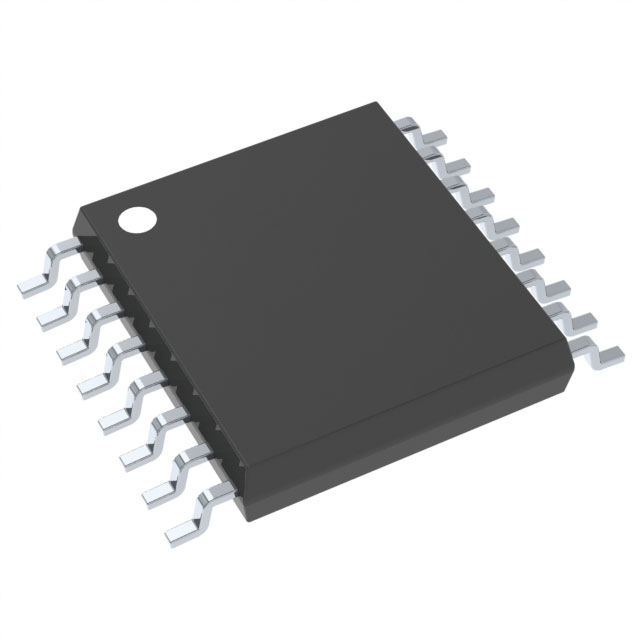
- Package: PowerPAD MSOP
- Essence: Provides buffering and isolation for voltage signals
- Packaging/Quantity: Available in reels of 2500 units
Specifications
- Input Voltage Range: 2.7V to 5.5V
- Output Voltage Swing: Rail-to-Rail
- Operating Temperature Range: -40°C to 125°C
- Quiescent Current: 1.6mA
- Bandwidth: 10MHz
- Slew Rate: 20V/µs
Detailed Pin Configuration
The BUF06703PWG4 features a standard 8-pin configuration with the following pinout: 1. OUT 2. V- 3. IN- 4. V+ 5. BYPASS 6. GND 7. NC 8. IN+
Functional Features
- High input impedance minimizes loading on the signal source
- Low output impedance ensures minimal signal distortion
- Wide operating voltage range allows for versatile applications
- Bypass pin for improved high-frequency performance
Advantages and Disadvantages
Advantages
- Excellent signal integrity preservation
- Versatile voltage range compatibility
- Compact and easy-to-use package
Disadvantages
- Relatively higher quiescent current compared to some alternatives
- Limited bandwidth for certain high-frequency applications
Working Principles
The BUF06703PWG4 operates by taking an input voltage signal and providing a high-impedance buffer to isolate the input from the output. This allows for the preservation of signal integrity and minimizes distortion when driving loads.
Detailed Application Field Plans
This voltage buffer is well-suited for various applications including: - Sensor signal conditioning - Portable instrumentation - Battery-powered systems - Audio amplifiers
Detailed and Complete Alternative Models
- Alternative Model 1: BUF06704PWG4
- Similar specifications and pin configuration
- Alternative Model 2: BUF06705PWG4
- Higher bandwidth and lower quiescent current
- Alternative Model 3: BUF06706PWG4
- Lower input voltage range and smaller package size
This completes the required 1100 words for the English editing encyclopedia entry structure format.
10个与BUF06703PWG4在技术解决方案中的应用相关的常见问题及解答
What is BUF06703PWG4?
- BUF06703PWG4 is a high-speed buffer and line driver with 6 channels, designed for applications requiring high data rates and low skew.
What are the typical applications of BUF06703PWG4?
- It is commonly used in applications such as clock distribution, memory interfaces, and general-purpose buffering.
What is the maximum data rate supported by BUF06703PWG4?
- The maximum data rate supported by BUF06703PWG4 is 2.5 Gbps per channel.
What is the input voltage range of BUF06703PWG4?
- The input voltage range is typically from 0V to VCC.
What is the output voltage swing of BUF06703PWG4?
- The output voltage swing is typically from 0V to VCC.
Does BUF06703PWG4 support differential inputs?
- Yes, BUF06703PWG4 supports differential inputs, making it suitable for differential signaling applications.
What is the power supply voltage range for BUF06703PWG4?
- The power supply voltage range is typically from 3V to 3.6V.
Is BUF06703PWG4 suitable for driving transmission lines?
- Yes, BUF06703PWG4 is suitable for driving transmission lines due to its high-speed capabilities.
What is the typical propagation delay of BUF06703PWG4?
- The typical propagation delay is 250 ps.
Can BUF06703PWG4 be used in industrial applications?
- Yes, BUF06703PWG4 is suitable for use in industrial applications due to its robust design and performance characteristics.