

DAC101S101QCMK/NOPB
Product Overview
Category: Digital-to-Analog Converter (DAC)
Use: The DAC101S101QCMK/NOPB is a high-performance, low-power, 10-bit digital-to-analog converter designed for various applications that require precise analog output generation. It is commonly used in audio systems, instrumentation, industrial control systems, and communication devices.
Characteristics: - High resolution: The DAC101S101QCMK/NOPB provides a 10-bit resolution, allowing for fine-grained analog output. - Low power consumption: This DAC operates at a low power supply voltage, making it suitable for battery-powered devices. - Fast settling time: The device offers a fast settling time, ensuring accurate and responsive analog output. - Small package size: The DAC101S101QCMK/NOPB comes in a compact package, enabling space-efficient designs. - Robust performance: It exhibits excellent linearity, low glitch energy, and low integral non-linearity, ensuring reliable and precise analog output.
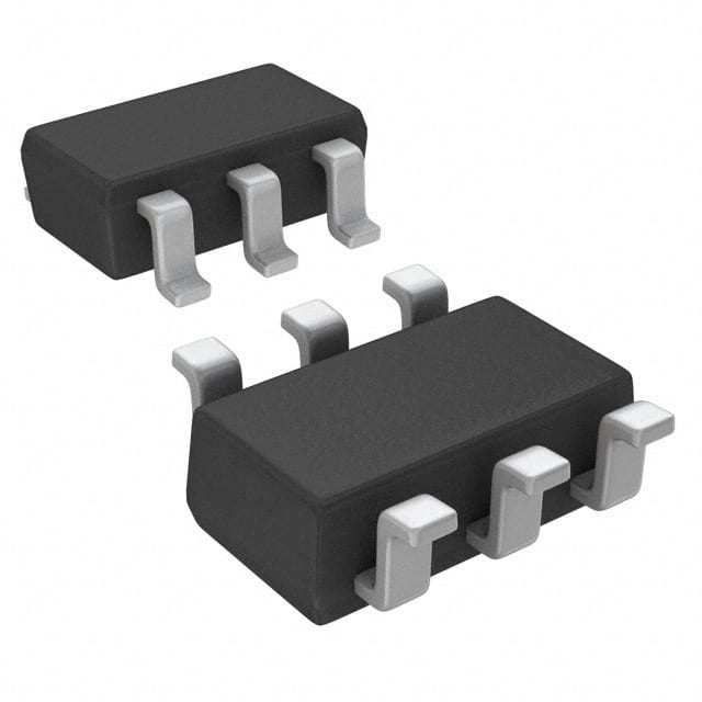
Package: The DAC101S101QCMK/NOPB is available in a small form-factor package, such as a QFN (Quad Flat No-leads) package. This package type offers good thermal dissipation and ease of integration into circuit boards.
Packaging/Quantity: The DAC101S101QCMK/NOPB is typically supplied in reels or trays, depending on the manufacturer's packaging standards. The quantity per reel or tray may vary, but it is commonly available in quantities of 250 or 1000 units.
Specifications
- Resolution: 10 bits
- Supply Voltage: 2.7V to 5.5V
- Output Range: 0V to Vref
- Settling Time: <10µs
- Operating Temperature Range: -40°C to +85°C
- Power Consumption: <1mW
Detailed Pin Configuration
The DAC101S101QCMK/NOPB has the following pin configuration:
- VDD: Power supply voltage input
- GND: Ground reference
- DIN: Digital input for data
- CS: Chip select input
- SCLK: Serial clock input
- VREF: Reference voltage input
- OUT: Analog output
Functional Features
- Serial Interface: The DAC101S101QCMK/NOPB utilizes a serial interface (SPI or I2C) for easy integration with microcontrollers and other digital systems.
- Internal Voltage Reference: It incorporates an internal voltage reference, eliminating the need for an external reference source.
- Power-On Reset: The device includes a power-on reset circuitry that ensures proper initialization upon power-up.
- Low Glitch Energy: The DAC exhibits low glitch energy, minimizing unwanted transients during analog output transitions.
Advantages and Disadvantages
Advantages: - High resolution enables precise analog output generation. - Low power consumption makes it suitable for battery-powered applications. - Fast settling time ensures accurate and responsive analog output. - Small package size allows for space-efficient designs. - Robust performance guarantees reliable and precise analog output.
Disadvantages: - Limited resolution compared to higher-bit DACs. - May require additional external components for specific applications.
Working Principles
The DAC101S101QCMK/NOPB operates by converting digital input data into corresponding analog output voltages. It utilizes a digital-to-analog conversion technique, where the binary input code is translated into an analog voltage level. The internal circuitry of the DAC performs this conversion using a combination of resistors, switches, and amplifiers.
Upon receiving digital input data, the DAC processes the information and generates an analog output voltage proportional to the input code. This analog voltage can be used as a control signal or as an accurate representation of the digital data in various applications.
Detailed Application Field Plans
The DAC101S101QCMK/NOPB finds application in several fields, including:
- Audio Systems: It is used in audio equipment for generating precise analog signals, such as volume control and tone generation.
- Instrumentation: The DAC is employed in measurement and testing instruments where accurate analog outputs are required.
- Industrial Control Systems: It plays a vital role in industrial automation systems, providing analog control signals for actuators and sensors.
- Communication Devices: The DAC is utilized in communication devices for generating analog signals used in modulation and demodulation processes.
Detailed and Complete Alternative Models
- DAC102S085CIMM/NOPB
- DAC0832LCN/NOPB
- MAX531BCSD+T
- MCP4725A0T-E/CH
These alternative models offer similar functionality and performance characteristics to the DAC101S101QCMK/NOPB and can be considered
10个与DAC101S101QCMK/NOPB在技术解决方案中的应用相关的常见问题及解答
What is the operating voltage range of DAC101S101QCMK/NOPB?
- The operating voltage range of DAC101S101QCMK/NOPB is 2.7V to 5.5V.What is the resolution of DAC101S101QCMK/NOPB?
- DAC101S101QCMK/NOPB has a resolution of 10 bits.Can DAC101S101QCMK/NOPB be used in industrial control applications?
- Yes, DAC101S101QCMK/NOPB is suitable for industrial control applications.What is the output voltage range of DAC101S101QCMK/NOPB?
- The output voltage range of DAC101S101QCMK/NOPB is 0V to Vref.Is DAC101S101QCMK/NOPB compatible with I2C interface?
- Yes, DAC101S101QCMK/NOPB is compatible with I2C interface.Can DAC101S101QCMK/NOPB be used in automotive electronics?
- Yes, DAC101S101QCMK/NOPB is suitable for automotive electronics applications.What is the typical settling time of DAC101S101QCMK/NOPB?
- The typical settling time of DAC101S101QCMK/NOPB is 6µs.Does DAC101S101QCMK/NOPB have an internal reference voltage?
- No, DAC101S101QCMK/NOPB requires an external reference voltage.Can DAC101S101QCMK/NOPB be used in battery-powered devices?
- Yes, DAC101S101QCMK/NOPB is suitable for battery-powered devices due to its low power consumption.What is the temperature range for operation of DAC101S101QCMK/NOPB?
- DAC101S101QCMK/NOPB can operate within a temperature range of -40°C to 125°C.