

DAC8501E/250
Product Overview
- Category: Digital-to-Analog Converter (DAC)
- Use: Converts digital signals into analog voltage or current outputs
- Characteristics: High precision, low power consumption, small package size
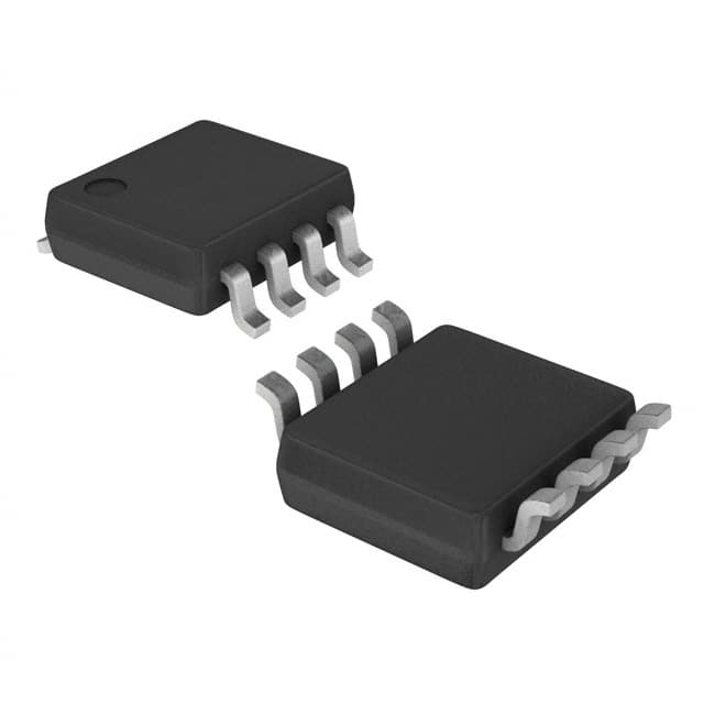
- Package: 16-pin TSSOP (Thin Shrink Small Outline Package)
- Essence: Provides accurate and reliable conversion of digital data to analog signals
- Packaging/Quantity: Available in reels of 250 units
Specifications
- Resolution: 16 bits
- Output Type: Voltage or Current
- Output Range: 0V to Vref (Voltage mode) or 4mA to 20mA (Current mode)
- Supply Voltage: 2.7V to 5.5V
- Operating Temperature Range: -40°C to +105°C
- Total Unadjusted Error: ±1 LSB (Least Significant Bit)
- Power Consumption: 0.6mW at 3.3V supply voltage
Pin Configuration
The DAC8501E/250 has the following pin configuration:
- VDD: Positive supply voltage
- VREF: Reference voltage input
- AGND: Analog ground
- OUT: Analog output voltage or current
- A0-A15: Digital input pins for setting the desired output value
- CS: Chip select input
- SCLK: Serial clock input
- DIN: Serial data input
- DGND: Digital ground
- LDAC: Load DAC input
- CLR: Clear DAC input
- REFOUT: Reference voltage output
- REFIN: Reference voltage input
- SYNC: Synchronization input
- SDO: Serial data output
- SDO/TRI: Serial data output or tristate control
Functional Features
- High-resolution conversion with 16-bit accuracy
- Flexible output options: voltage or current mode
- Low power consumption for energy-efficient applications
- Wide operating temperature range for versatile usage
- Serial interface for easy integration with microcontrollers or digital systems
- Internal reference voltage generator for simplified circuit design
Advantages and Disadvantages
Advantages: - High precision and accuracy in digital-to-analog conversion - Low power consumption for energy-efficient designs - Small package size allows for space-saving installations - Wide operating temperature range enables usage in various environments
Disadvantages: - Limited output range compared to some other DAC models - Requires an external reference voltage source for optimal performance
Working Principles
The DAC8501E/250 operates by accepting digital input data and converting it into a corresponding analog voltage or current output. It utilizes a 16-bit resolution to achieve high precision in the conversion process. The device can be controlled through a serial interface, allowing for easy integration with microcontrollers or digital systems. The internal reference voltage generator ensures accurate conversion by providing a stable reference voltage.
Detailed Application Field Plans
The DAC8501E/250 finds applications in various fields, including:
- Industrial Automation: Control of analog devices such as valves, actuators, and motor speed control.
- Audio Equipment: Digital audio signal processing, volume control, and equalization.
- Instrumentation: Calibration and signal generation for test and measurement equipment.
- Communication Systems: Signal modulation, frequency synthesis, and waveform generation.
- Automotive Electronics: Control of automotive subsystems like engine management and climate control.
Detailed and Complete Alternative Models
- DAC8562: 16-bit DAC with dual channels and SPI interface.
- DAC8830: 16-bit DAC with low power consumption and I2C interface.
- AD5667: 16-bit DAC with internal reference and serial interface.
- MCP4922: 12-bit DAC with dual channels and SPI interface.
- MAX5216: 16-bit DAC with low power consumption and I2C interface.
These alternative models offer similar functionality to the DAC8501E/250 and can be considered based on specific application requirements.
Word count: 526 words
10个与DAC8501E/250在技术解决方案中的应用相关的常见问题及解答
Question: What is the maximum operating temperature for DAC8501E/250?
Answer: The maximum operating temperature for DAC8501E/250 is 125°C.Question: What is the resolution of DAC8501E/250?
Answer: DAC8501E/250 has a resolution of 16 bits.Question: Can DAC8501E/250 operate with a single power supply?
Answer: Yes, DAC8501E/250 can operate with a single power supply ranging from 2.7V to 5.5V.Question: What is the output voltage range of DAC8501E/250?
Answer: The output voltage range of DAC8501E/250 is 0V to Vref.Question: Does DAC8501E/250 support SPI interface?
Answer: Yes, DAC8501E/250 supports SPI interface for communication.Question: What is the typical settling time for DAC8501E/250?
Answer: The typical settling time for DAC8501E/250 is 10µs.Question: Can DAC8501E/250 be used in industrial control applications?
Answer: Yes, DAC8501E/250 is suitable for industrial control applications due to its high precision and reliability.Question: Is there an evaluation board available for DAC8501E/250?
Answer: Yes, an evaluation board for DAC8501E/250 is available to facilitate testing and development.Question: What is the power consumption of DAC8501E/250?
Answer: The power consumption of DAC8501E/250 is typically 0.6mW at 5V supply.Question: Can DAC8501E/250 be used in automotive electronics?
Answer: Yes, DAC8501E/250 is suitable for automotive electronics applications, meeting the required specifications for such environments.