

SN74LV373ADBR
Product Overview
Category
SN74LV373ADBR belongs to the category of integrated circuits (ICs).
Use
This product is commonly used in digital systems for data storage and transfer.
Characteristics
- Low-voltage operation
- High-speed performance
- D-type transparent latch
- 3-state outputs
Package
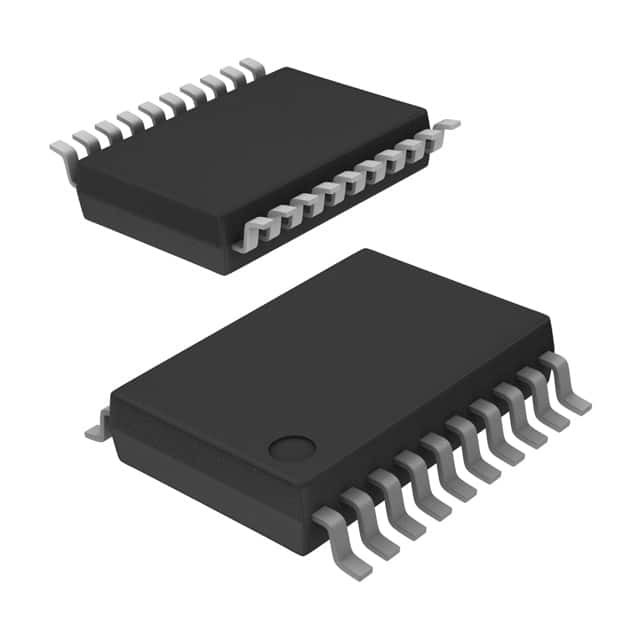
SN74LV373ADBR is available in a small-outline package (SOIC) with 20 pins.
Essence
The essence of SN74LV373ADBR lies in its ability to store and transfer data efficiently within digital systems.
Packaging/Quantity
This product is typically packaged in reels or tubes, with a quantity of 2500 units per reel/tube.
Specifications
- Supply voltage: 2.0V to 5.5V
- Input voltage range: 0V to VCC
- Output voltage range: 0V to VCC
- Operating temperature range: -40°C to +85°C
- Maximum propagation delay: 6 ns
Detailed Pin Configuration
- OE (Output Enable)
- LE (Latch Enable)
- D0-D7 (Data Inputs/Outputs)
- GND (Ground)
- Q0-Q7 (Data Outputs)
- VCC (Supply Voltage)
Functional Features
- D-type transparent latch with 3-state outputs
- Latch enable input for storing data
- Output enable input for controlling the output state
- Wide operating voltage range for compatibility with various systems
Advantages and Disadvantages
Advantages
- Low-voltage operation allows for reduced power consumption
- High-speed performance enables efficient data transfer
- 3-state outputs provide flexibility in connecting multiple devices
Disadvantages
- Limited number of data inputs/outputs (8 bits)
- Not suitable for applications requiring higher data storage capacity
Working Principles
SN74LV373ADBR operates based on the principles of latch-based data storage and transfer. When the latch enable (LE) input is high, the data inputs (D0-D7) are latched and stored. The stored data can then be outputted through the data outputs (Q0-Q7) when the output enable (OE) input is also high.
Detailed Application Field Plans
SN74LV373ADBR finds extensive use in various digital systems, including but not limited to: - Microcontrollers - Data communication devices - Memory modules - Industrial automation systems
Detailed and Complete Alternative Models
- SN74LV374ADBR: Similar to SN74LV373ADBR, but with an additional clock input for synchronous operation.
- SN74HC373N: A compatible alternative from a different series, offering similar functionality.
Please note that these alternative models may have slight variations in specifications and pin configurations.
Word count: 335 words
10个与SN74LV373ADBR在技术解决方案中的应用相关的常见问题及解答
Sure! Here are 10 common questions and answers related to the application of SN74LV373ADBR:
Q: What is SN74LV373ADBR? A: SN74LV373ADBR is a type of octal transparent latch with 3-state outputs, commonly used in digital systems.
Q: What is the maximum operating voltage for SN74LV373ADBR? A: The maximum operating voltage for SN74LV373ADBR is 5.5V.
Q: How many latch outputs does SN74LV373ADBR have? A: SN74LV373ADBR has 8 latch outputs, making it suitable for applications requiring multiple data storage.
Q: Can SN74LV373ADBR be used as a bidirectional buffer? A: No, SN74LV373ADBR is not designed for bidirectional buffering. It is primarily used for data storage and transfer.
Q: What is the typical propagation delay of SN74LV373ADBR? A: The typical propagation delay of SN74LV373ADBR is around 6 ns.
Q: Can SN74LV373ADBR handle high-speed data transfers? A: Yes, SN74LV373ADBR is capable of handling high-speed data transfers due to its low propagation delay and high-speed operation.
Q: Is SN74LV373ADBR compatible with TTL logic levels? A: Yes, SN74LV373ADBR is compatible with both TTL and CMOS logic levels, making it versatile for various digital systems.
Q: Can SN74LV373ADBR be cascaded to increase the number of latch outputs? A: Yes, SN74LV373ADBR can be cascaded by connecting the output of one latch to the input of another, allowing for expansion of latch outputs.
Q: What is the maximum output current that SN74LV373ADBR can sink/source? A: SN74LV373ADBR can sink/source up to 12 mA of current per output pin.
Q: Can SN74LV373ADBR be used in battery-powered applications? A: Yes, SN74LV373ADBR can be used in battery-powered applications as it operates at low power supply voltages and has low power consumption.
Please note that these answers are general and may vary depending on specific application requirements.