

XC6124D540MR-G
Product Overview
Category
XC6124D540MR-G belongs to the category of voltage regulators.
Use
It is primarily used for regulating voltage in electronic circuits.
Characteristics
- Voltage regulation capability
- Compact size
- Low power consumption
- High efficiency
Package
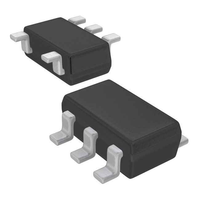
XC6124D540MR-G comes in a small surface-mount package.
Essence
The essence of XC6124D540MR-G lies in its ability to provide stable and regulated voltage output.
Packaging/Quantity
XC6124D540MR-G is typically packaged in reels or tubes, with a quantity of 3000 units per reel/tube.
Specifications
- Input Voltage Range: 2.5V - 6.0V
- Output Voltage: 5.4V ±2%
- Maximum Output Current: 200mA
- Dropout Voltage: 150mV @ 100mA
- Quiescent Current: 30μA (typical)
- Operating Temperature Range: -40°C to +85°C
Detailed Pin Configuration
XC6124D540MR-G has the following pin configuration:
- VIN: Input voltage pin
- GND: Ground pin
- VOUT: Output voltage pin
- CE: Chip enable pin
Functional Features
- Voltage regulation: XC6124D540MR-G ensures a stable output voltage regardless of input voltage fluctuations.
- Overcurrent protection: It incorporates overcurrent protection to safeguard connected devices.
- Low quiescent current: The low quiescent current minimizes power consumption when the device is idle.
- Thermal shutdown: It includes thermal shutdown protection to prevent overheating.
Advantages and Disadvantages
Advantages
- Compact size allows for easy integration into space-constrained designs.
- High efficiency results in minimal power loss.
- Wide operating temperature range enables usage in various environments.
Disadvantages
- Limited maximum output current may not be suitable for high-power applications.
- Dropout voltage may affect performance in low input voltage scenarios.
Working Principles
XC6124D540MR-G operates by comparing the output voltage with a reference voltage. It adjusts the internal circuitry to maintain a stable output voltage, compensating for any changes in the input voltage or load conditions.
Detailed Application Field Plans
XC6124D540MR-G finds applications in various electronic devices and systems, including but not limited to: - Mobile phones - Portable media players - Digital cameras - Wearable devices - IoT devices
Detailed and Complete Alternative Models
Some alternative models that can be considered as alternatives to XC6124D540MR-G are: - XC6206P542MR-G - XC6220B542MR-G - XC6219B542MR-G - XC6221B542MR-G
These models offer similar voltage regulation capabilities and package options, providing flexibility in design choices.
In conclusion, XC6124D540MR-G is a compact voltage regulator with excellent voltage regulation characteristics. Its small size, low power consumption, and high efficiency make it suitable for a wide range of applications. However, designers should consider its limitations in terms of maximum output current and dropout voltage when selecting this device for specific projects.
10个与XC6124D540MR-G在技术解决方案中的应用相关的常见问题及解答
Sure! Here are 10 common questions and answers related to the application of XC6124D540MR-G in technical solutions:
Q: What is XC6124D540MR-G? A: XC6124D540MR-G is a voltage detector IC (integrated circuit) manufactured by Torex Semiconductor. It is used to monitor the voltage level in electronic circuits.
Q: What is the operating voltage range of XC6124D540MR-G? A: The operating voltage range of XC6124D540MR-G is from 0.8V to 6.0V.
Q: What is the output type of XC6124D540MR-G? A: XC6124D540MR-G has an open-drain output type, which means it can sink current but cannot source current.
Q: What is the typical quiescent current consumption of XC6124D540MR-G? A: The typical quiescent current consumption of XC6124D540MR-G is 1.0µA.
Q: Can XC6124D540MR-G be used for overvoltage detection? A: No, XC6124D540MR-G is specifically designed for undervoltage detection only.
Q: What is the hysteresis voltage of XC6124D540MR-G? A: The hysteresis voltage of XC6124D540MR-G is typically 50mV.
Q: What is the maximum reset delay time of XC6124D540MR-G? A: The maximum reset delay time of XC6124D540MR-G is typically 200ms.
Q: Can XC6124D540MR-G be used in automotive applications? A: Yes, XC6124D540MR-G is AEC-Q100 qualified and suitable for automotive applications.
Q: What is the operating temperature range of XC6124D540MR-G? A: The operating temperature range of XC6124D540MR-G is from -40°C to +85°C.
Q: Is XC6124D540MR-G available in a surface-mount package? A: Yes, XC6124D540MR-G is available in a small SOT-25 package, which is suitable for surface-mount assembly.
Please note that these answers are based on general information about XC6124D540MR-G and may vary depending on specific datasheet specifications or application requirements.