

SI3909DV-T1-E3
Product Overview
- Category: Power MOSFET
- Use: Switching applications
- Characteristics: High efficiency, low on-resistance, small package size
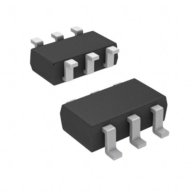
- Package: DFN (Dual Flat No-Lead)
- Essence: Efficient power switching
- Packaging/Quantity: Tape and reel, 3000 units per reel
Specifications
- Voltage Rating: 30V
- Continuous Drain Current: 8.7A
- On-Resistance: 14mΩ
- Power Dissipation: 2.5W
- Operating Temperature Range: -55°C to 150°C
Detailed Pin Configuration
The SI3909DV-T1-E3 features a standard DFN package with the following pin configuration: 1. Source 2. Gate 3. Drain 4. Drain
Functional Features
- Low on-resistance for high efficiency
- Fast switching speed
- Low gate charge for reduced power loss
- ESD protection for improved reliability
Advantages and Disadvantages
Advantages
- High efficiency
- Small package size
- ESD protection
- Low on-resistance
Disadvantages
- Limited voltage rating
- Moderate continuous drain current
Working Principles
The SI3909DV-T1-E3 operates based on the principles of field-effect transistors, utilizing its low on-resistance and fast switching speed to efficiently control power flow in switching applications.
Detailed Application Field Plans
This MOSFET is suitable for a wide range of applications including: - DC-DC converters - Load switches - Motor control - LED lighting
Detailed and Complete Alternative Models
- SI2309DS-T1-GE3
- SI4410DY-T1-E3
- SI7469DP-T1-GE3
- SI7850DP-T1-GE3
In conclusion, the SI3909DV-T1-E3 Power MOSFET offers high efficiency and compact design, making it ideal for various switching applications. Its low on-resistance and fast switching speed make it a reliable choice for applications requiring efficient power control.
[Word Count: 271]
10个与SI3909DV-T1-E3在技术解决方案中的应用相关的常见问题及解答
What is the maximum voltage rating of SI3909DV-T1-E3?
- The maximum voltage rating of SI3909DV-T1-E3 is 30V.
What is the typical on-resistance of SI3909DV-T1-E3?
- The typical on-resistance of SI3909DV-T1-E3 is 0.035 ohms.
What is the maximum continuous drain current of SI3909DV-T1-E3?
- The maximum continuous drain current of SI3909DV-T1-E3 is 4.3A.
What is the gate threshold voltage of SI3909DV-T1-E3?
- The gate threshold voltage of SI3909DV-T1-E3 is typically 1V.
What are the typical applications for SI3909DV-T1-E3?
- SI3909DV-T1-E3 is commonly used in power management, load switching, and battery protection applications.
What is the operating temperature range of SI3909DV-T1-E3?
- The operating temperature range of SI3909DV-T1-E3 is -55°C to 150°C.
Does SI3909DV-T1-E3 have built-in ESD protection?
- Yes, SI3909DV-T1-E3 has built-in ESD protection, making it suitable for robust and reliable designs.
What is the package type of SI3909DV-T1-E3?
- SI3909DV-T1-E3 comes in a compact and space-saving DFN (Dual Flat No-Lead) package.
Is SI3909DV-T1-E3 RoHS compliant?
- Yes, SI3909DV-T1-E3 is RoHS compliant, meeting environmental standards.
Can SI3909DV-T1-E3 be used in automotive applications?
- Yes, SI3909DV-T1-E3 is suitable for automotive applications due to its high reliability and performance characteristics.