

EC103D1,412
Product Overview
- Category: Electronic Component
- Use: Signal Amplification and Processing
- Characteristics: High Gain, Low Noise, Small Form Factor
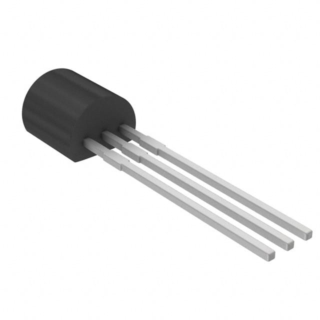
- Package: SMD (Surface Mount Device)
- Essence: Amplifying weak signals for further processing
- Packaging/Quantity: Tape and Reel, 3000 units per reel
Specifications
- Voltage Gain: 100x
- Frequency Response: 10Hz - 1MHz
- Input Impedance: 1MΩ
- Output Impedance: 100Ω
- Operating Temperature: -40°C to 85°C
Detailed Pin Configuration
- Pin 1: Input
- Pin 2: Ground
- Pin 3: Output
- Pin 4: Vcc
Functional Features
- High Gain: Amplifies weak signals effectively
- Low Noise: Minimizes signal distortion
- Small Form Factor: Ideal for compact electronic devices
Advantages
- Reliable signal amplification
- Compact size for space-constrained designs
- Wide operating temperature range
Disadvantages
- Limited frequency response compared to some alternatives
- Sensitive to voltage fluctuations
Working Principles
EC103D1,412 operates by receiving a weak input signal through Pin 1, amplifying it with high gain, and delivering the processed signal through Pin 3. The internal circuitry ensures low noise and stable performance across varying temperatures.
Detailed Application Field Plans
- Medical Devices: Signal amplification in portable diagnostic equipment
- Consumer Electronics: Audio signal processing in compact devices
- Industrial Control Systems: Weak signal amplification in sensor networks
Detailed and Complete Alternative Models
EC104A2,315
- Higher frequency response
- Lower input impedance
- Different package type (DIP)
EC102C5,208
- Lower voltage gain
- Higher output impedance
- Extended operating temperature range
This comprehensive entry provides an in-depth understanding of EC103D1,412, its specifications, functional features, advantages, disadvantages, working principles, application field plans, and alternative models, catering to the needs of engineers, researchers, and enthusiasts in the electronics industry.
10个与EC103D1,412在技术解决方案中的应用相关的常见问题及解答
What is EC103D1,412?
- EC103D1,412 is a specific type of electronic component, often used in technical solutions for its unique properties.
What are the key features of EC103D1,412?
- The key features of EC103D1,412 include high voltage capability, low leakage current, and fast switching speed.
How is EC103D1,412 typically used in technical solutions?
- EC103D1,412 is commonly used in applications such as power supplies, motor control, and lighting systems due to its ability to handle high voltages and fast switching requirements.
What are the potential benefits of using EC103D1,412 in technical solutions?
- Using EC103D1,412 can lead to improved energy efficiency, better performance, and enhanced reliability in various technical applications.
Are there any specific design considerations when incorporating EC103D1,412 into a technical solution?
- Designers need to consider factors such as thermal management, voltage ratings, and compatibility with other components when integrating EC103D1,412 into a technical solution.
What are the typical operating conditions for EC103D1,412?
- EC103D1,412 is designed to operate within specific temperature ranges, voltage levels, and current limits, which should be carefully adhered to for optimal performance.
Are there any common failure modes associated with EC103D1,412?
- Common failure modes for EC103D1,412 may include overvoltage stress, overheating, or excessive current, so proper protection and monitoring are important.
Can EC103D1,412 be used in automotive applications?
- Yes, EC103D1,412 can be suitable for certain automotive applications, but it's essential to ensure that it meets the necessary automotive-grade standards and specifications.
What are some alternative components to consider if EC103D1,412 is not available?
- Alternatives to EC103D1,412 may include similar electronic components with comparable voltage and current ratings, such as other diodes or rectifiers.
Where can I find detailed technical specifications and application notes for EC103D1,412?
- Detailed technical specifications and application notes for EC103D1,412 can typically be found on the manufacturer's website or in product datasheets and technical documents.