

XC3S1400A-4FGG676I
Product Overview
Category
The XC3S1400A-4FGG676I belongs to the category of Field-Programmable Gate Arrays (FPGAs).
Use
FPGAs are integrated circuits that can be programmed and reprogrammed to perform various digital functions. The XC3S1400A-4FGG676I is specifically designed for applications requiring high-performance logic capacity and flexibility.
Characteristics
- High logic capacity: The XC3S1400A-4FGG676I offers a large number of configurable logic blocks, allowing for complex digital designs.
- Flexibility: With its programmable nature, this FPGA provides the ability to implement custom logic functions and adapt to changing requirements.
- Fast performance: The XC3S1400A-4FGG676I operates at high clock frequencies, enabling rapid data processing.
- Low power consumption: This FPGA incorporates power-saving features, making it suitable for energy-efficient applications.
Package
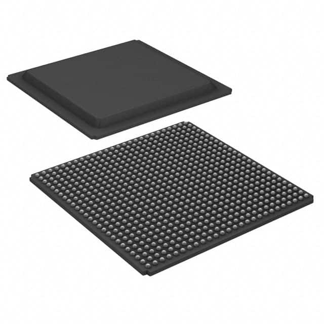
The XC3S1400A-4FGG676I comes in a FG676 package, which refers to a fine-pitch grid array with 676 pins.
Essence
The essence of the XC3S1400A-4FGG676I lies in its ability to provide a highly configurable and flexible platform for digital circuit design and implementation.
Packaging/Quantity
This FPGA is typically packaged individually and is available in various quantities depending on the manufacturer and distributor.
Specifications
- Logic cells: 1,400
- Flip-flops: 2,800
- Block RAM: 576 Kb
- Maximum user I/Os: 500
- Operating voltage: 1.2V
- Operating temperature range: -40°C to +100°C
- Package dimensions: 27mm x 27mm
Detailed Pin Configuration
The XC3S1400A-4FGG676I has a total of 676 pins, each serving a specific purpose in the circuit design. The pin configuration can be found in the manufacturer's datasheet or reference manual.
Functional Features
- Configurable logic blocks: The FPGA contains numerous configurable logic blocks that can be interconnected to implement complex digital functions.
- Programmable interconnects: The XC3S1400A-4FGG676I offers a flexible interconnect structure, allowing for the routing of signals between different logic elements.
- Dedicated input/output resources: This FPGA provides dedicated input/output pins for interfacing with external devices and peripherals.
- On-chip memory: The integrated block RAM allows for efficient storage and retrieval of data within the FPGA itself.
- Clock management: The XC3S1400A-4FGG676I includes built-in clock management resources, enabling precise timing control.
Advantages and Disadvantages
Advantages
- High flexibility and reconfigurability
- Large logic capacity for complex designs
- Fast performance and high-speed data processing
- Low power consumption compared to traditional ASICs
- Cost-effective solution for prototyping and low-volume production
Disadvantages
- Limited maximum operating frequency compared to dedicated ASICs
- Higher cost per unit compared to mass-produced ASICs
- Steeper learning curve for programming and utilizing FPGAs effectively
Working Principles
FPGAs like the XC3S1400A-4FGG676I operate based on the principle of configurable logic. The device consists of an array of programmable logic blocks interconnected through configurable routing resources. These logic blocks can be programmed to perform various digital functions by configuring their internal look-up tables, flip-flops, and interconnections. The resulting circuit configuration is stored in non-volatile memory within the FPGA and can be reprogrammed as needed.
Detailed Application Field Plans
The XC3S1400A-4FGG676I finds applications in various fields, including:
- Communications: Used in networking equipment, routers, and switches for high-speed data processing and protocol handling.
- Industrial automation: Employed in control systems, robotics, and machine vision applications for real-time processing and control.
- Aerospace and defense: Utilized in radar systems, avionics, and military communication devices for their flexibility and performance.
- Medical devices: Integrated into medical imaging systems, patient monitoring equipment, and diagnostic instruments for signal processing and analysis.
- Automotive electronics: Applied in advanced driver assistance systems (ADAS), infotainment systems, and engine control units for their versatility and adaptability.
Detailed and Complete Alternative Models
- XC7A35T-1CPG236C
- EP4CE6E22C8N
- LCMXO2-1200HC-4TG100C
- MAX 10M08SAU169C8G
- ECP5-12F
10个与XC3S1400A-4FGG676I在技术解决方案中的应用相关的常见问题及解答
Sure! Here are 10 common questions and answers related to the application of XC3S1400A-4FGG676I in technical solutions:
Q: What is XC3S1400A-4FGG676I? A: XC3S1400A-4FGG676I is a field-programmable gate array (FPGA) manufactured by Xilinx.
Q: What are the key features of XC3S1400A-4FGG676I? A: Some key features include 1400K system gates, 192 I/O pins, 4-input look-up tables, and a maximum operating frequency of 400 MHz.
Q: What are the typical applications of XC3S1400A-4FGG676I? A: XC3S1400A-4FGG676I is commonly used in various technical solutions such as digital signal processing, high-speed data communication, industrial automation, and embedded systems.
Q: How can XC3S1400A-4FGG676I be programmed? A: XC3S1400A-4FGG676I can be programmed using Xilinx's Vivado Design Suite or other compatible programming tools.
Q: What is the power supply requirement for XC3S1400A-4FGG676I? A: The recommended power supply voltage for XC3S1400A-4FGG676I is typically 1.2V, but it can operate within a range of 1.14V to 1.26V.
Q: Can XC3S1400A-4FGG676I interface with other devices? A: Yes, XC3S1400A-4FGG676I supports various communication interfaces such as SPI, I2C, UART, and Ethernet, allowing it to interface with other devices.
Q: What is the maximum operating temperature for XC3S1400A-4FGG676I? A: The maximum junction temperature for XC3S1400A-4FGG676I is 100°C, but it is recommended to operate within a range of -40°C to 85°C for reliable performance.
Q: Can XC3S1400A-4FGG676I be reprogrammed multiple times? A: Yes, XC3S1400A-4FGG676I is a reprogrammable FPGA, allowing it to be reprogrammed multiple times during its lifespan.
Q: Are there any development boards available for XC3S1400A-4FGG676I? A: Yes, Xilinx offers development boards like the Spartan-3A Evaluation Kit that can be used for prototyping and testing with XC3S1400A-4FGG676I.
Q: Where can I find more information about XC3S1400A-4FGG676I? A: You can refer to the official documentation provided by Xilinx, including datasheets, user guides, and application notes, for detailed information about XC3S1400A-4FGG676I.