

XCKU040-L1FBVA900I
Product Overview
- Category: Integrated Circuit (IC)
- Use: XCKU040-L1FBVA900I is a high-performance field-programmable gate array (FPGA) designed for various applications in the electronics industry.
- Characteristics: This FPGA offers advanced features such as high-speed performance, low power consumption, and reconfigurability. It is suitable for applications that require complex digital logic functions.
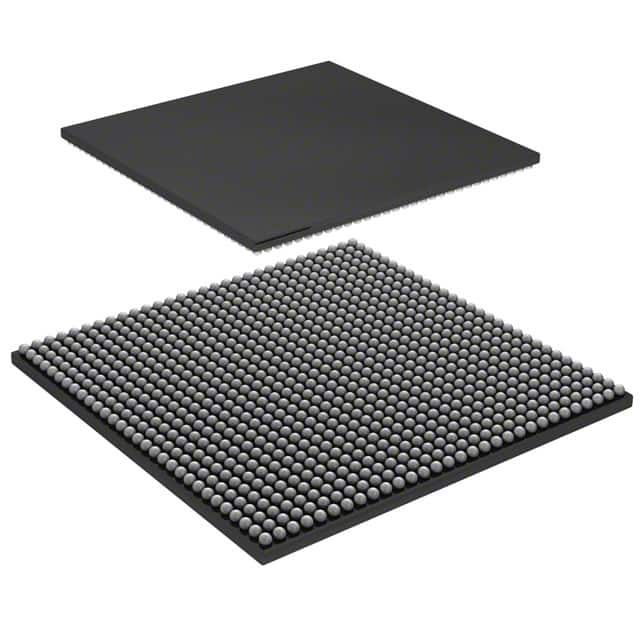
- Package: XCKU040-L1FBVA900I comes in a compact and durable package, ensuring easy integration into electronic systems.
- Essence: The essence of XCKU040-L1FBVA900I lies in its ability to provide flexible and customizable digital logic functionality, making it an essential component in many electronic devices.
- Packaging/Quantity: XCKU040-L1FBVA900I is typically packaged individually and is available in various quantities depending on the customer's requirements.
Specifications
- Logic Cells: 40,960
- DSP Slices: 2,520
- Block RAM: 4,860 Kb
- Clock Management Tiles: 80
- Transceivers: 16
- Operating Voltage: 0.95V - 1.05V
- Operating Temperature: -40°C to 100°C
- Package Type: Flip-Chip BGA
- Package Pins: 900
Detailed Pin Configuration
For a detailed pin configuration of XCKU040-L1FBVA900I, please refer to the manufacturer's datasheet or technical documentation.
Functional Features
- High-speed performance: XCKU040-L1FBVA900I offers fast processing capabilities, making it suitable for applications that require real-time data processing.
- Low power consumption: This FPGA is designed to minimize power consumption, making it energy-efficient and suitable for battery-powered devices.
- Reconfigurability: XCKU040-L1FBVA900I can be reprogrammed to adapt to changing requirements or to fix any design issues without the need for hardware changes.
Advantages
- Versatility: XCKU040-L1FBVA900I can be used in a wide range of applications, including telecommunications, automotive, aerospace, and industrial automation.
- High-performance: The FPGA's advanced architecture enables it to handle complex digital logic functions efficiently.
- Flexibility: With its reconfigurable nature, XCKU040-L1FBVA900I offers flexibility in design iterations and system upgrades.
Disadvantages
- Complexity: Working with FPGAs requires specialized knowledge and expertise, which may pose a challenge for beginners or those unfamiliar with digital design.
- Cost: FPGAs, including XCKU040-L1FBVA900I, can be relatively expensive compared to other integrated circuits, especially for small-scale projects.
Working Principles
XCKU040-L1FBVA900I operates based on the principles of configurable logic. It consists of an array of programmable logic cells interconnected through configurable routing resources. These logic cells can be programmed to implement various digital logic functions, allowing the FPGA to perform specific tasks as required by the application.
Detailed Application Field Plans
XCKU040-L1FBVA900I finds applications in various fields, including:
- Telecommunications: Used in high-speed data processing, signal modulation/demodulation, and network protocol implementation.
- Automotive: Employed in advanced driver assistance systems (ADAS), engine control units (ECUs), and infotainment systems.
- Aerospace: Utilized in avionics systems, flight control units, and satellite communication systems.
- Industrial Automation: Applied in programmable logic controllers (PLCs), motor control systems, and robotics.
Detailed and Complete Alternative Models
- XCKU060-L1FBVA900I: Similar to XCKU040-L1FBVA900I but with higher logic capacity.
- XCKU035-L1FBVA900I: Similar to XCKU040-L1FBVA900I but with lower logic capacity.
- XCKU100-L1FBVA900I: Similar to XCKU040-L1FBVA900I but with higher performance and additional features.
Note: The above alternative models are suggestions and may vary based on specific requirements and availability in the market.
Word count: 511 words
10个与XCKU040-L1FBVA900I在技术解决方案中的应用相关的常见问题及解答
Sure! Here are 10 common questions and answers related to the application of XCKU040-L1FBVA900I in technical solutions:
Q1: What is the XCKU040-L1FBVA900I? A1: The XCKU040-L1FBVA900I is a specific model of Xilinx's Kintex UltraScale FPGA family, designed for high-performance applications.
Q2: What are the key features of the XCKU040-L1FBVA900I? A2: Some key features include 40K logic cells, 900 MHz maximum operating frequency, integrated DSP slices, high-speed transceivers, and support for various I/O standards.
Q3: What are the typical applications of the XCKU040-L1FBVA900I? A3: The XCKU040-L1FBVA900I is commonly used in applications such as wireless communication systems, video processing, industrial automation, aerospace, and defense.
Q4: What programming languages can be used with the XCKU040-L1FBVA900I? A4: The XCKU040-L1FBVA900I can be programmed using hardware description languages (HDLs) like VHDL or Verilog, as well as higher-level synthesis tools like Vivado HLS.
Q5: How can I interface with external devices using the XCKU040-L1FBVA900I? A5: The XCKU040-L1FBVA900I provides various I/O standards, including LVCMOS, LVDS, and GTY/GTH transceivers, allowing you to interface with different types of external devices.
Q6: Can the XCKU040-L1FBVA900I handle real-time signal processing? A6: Yes, the XCKU040-L1FBVA900I is capable of real-time signal processing due to its high-performance architecture and integrated DSP slices.
Q7: How can I optimize power consumption with the XCKU040-L1FBVA900I? A7: The XCKU040-L1FBVA900I offers power optimization features such as clock gating, dynamic voltage scaling, and power-aware placement and routing techniques.
Q8: Can I use the XCKU040-L1FBVA900I in a multi-FPGA system? A8: Yes, the XCKU040-L1FBVA900I supports various communication protocols like AXI and PCIe, making it suitable for integration into multi-FPGA systems.
Q9: What development tools are available for programming the XCKU040-L1FBVA900I? A9: Xilinx provides Vivado Design Suite, which includes tools for FPGA synthesis, implementation, and debugging, along with IP cores and libraries.
Q10: Are there any reference designs or application notes available for the XCKU040-L1FBVA900I? A10: Yes, Xilinx provides a wide range of reference designs and application notes that can help you get started with the XCKU040-L1FBVA900I in different applications.
Please note that these answers are general and may vary depending on specific requirements and design considerations.