

MP4560DN-LF-Z
IC REG BUCK ADJ 2A
型号
MP4560DN-LF-Z
系列
-
零件状态
Active
包装
Tape & Reel (TR)
工作温度
-40°C ~ 125°C (TJ)
安装类型
Surface Mount
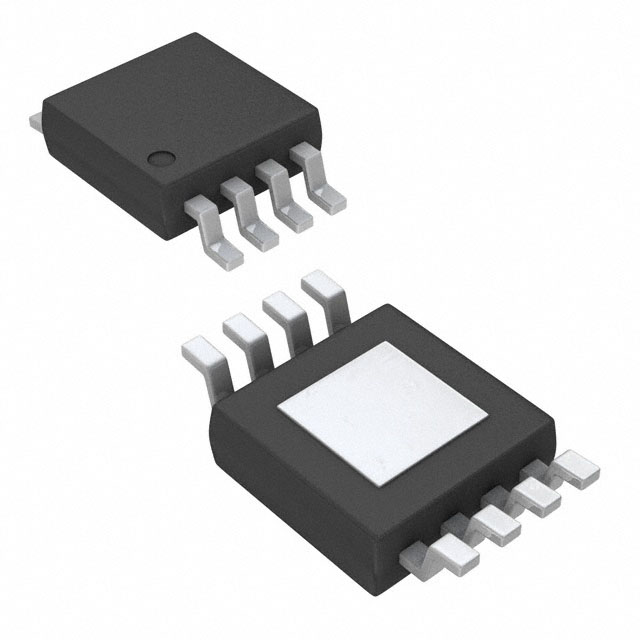
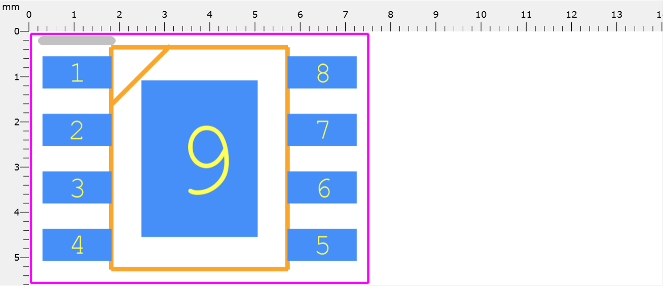
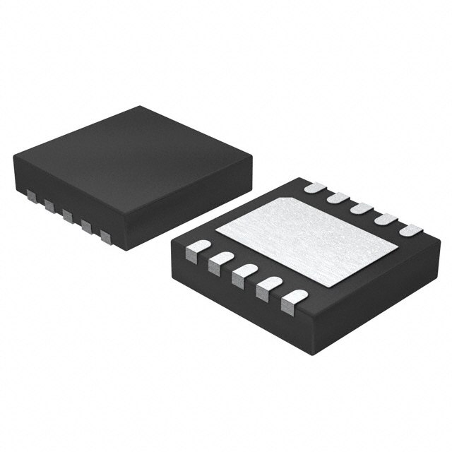
封装/箱体
8-SOIC (0.154", 3.90mm Width) Exposed Pad
电压 - 输入(最大)
55V
输出类型
Adjustable
供应商器件封装
8-SOIC-EP
功能
Step-Down
电流 - 输出
2A
频率 - 切换
Up to 2MHz
拓扑
Buck
输出配置
Positive
输出数量
1
电压 - 输出(最小/固定)
0.8V
电压 - 输出(最大)
52V
同步整流器
No
电压 - 输入(最小值)
3.8V
请求报价
请填写所有必填字段并点击“提交”,我们将在12小时内通过电子邮件与您联系。如果您有任何问题,请留言或发送电子邮件至 1943626632@qq.com,我们将尽快回复。
有货 36680 PCS
联系信息
more_pkgimg
more_schimg

more_3dimg
more_desctext
Switching Voltage Regulators 2A, 2MHz, 55V Step-Down Converter
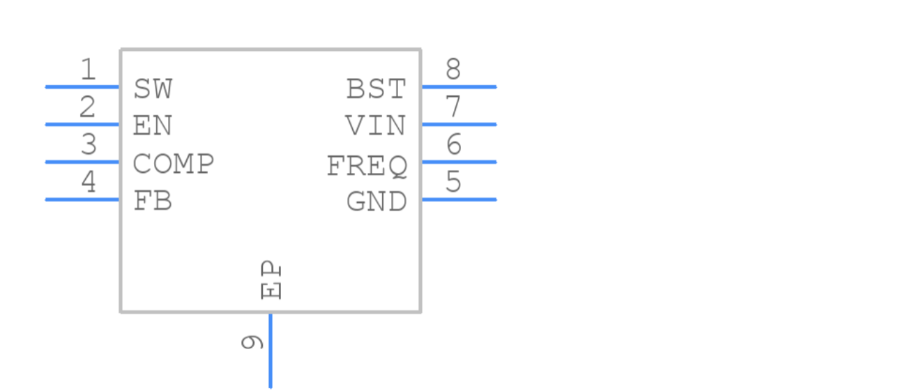
Pin Count--------9
Part Category--------Integrated Circuit
Package Category--------Small Outline Packages
Footprint Name--------Small Outline Packages - SOIC8
Pin Count--------9
Part Category--------Integrated Circuit
Package Category--------Small Outline Packages
Footprint Name--------Small Outline Packages - SOIC8
download_pdf
more_faq
MP4560DN-LF-Z Frequently Asked Questions (FAQs)
What is the recommended PCB layout for optimal thermal performance?
A 2-layer or 4-layer PCB with a solid ground plane and thermal vias is recommended. Keep the switching node (SW pin) away from sensitive analog nodes, and use a small, low-ESR output capacitor.
How do I optimize the compensation network for the voltage feedback loop?
Use the datasheet's recommended compensation network values as a starting point. Adjust RCOMP and CCOMP based on the specific application's output voltage, current, and desired transient response.
What is the maximum allowed input voltage ripple for reliable operation?
The MP4560DN-LF-Z can tolerate up to 10% input voltage ripple. Exceeding this may affect output regulation and device reliability.
Can I use a ceramic output capacitor instead of an electrolytic capacitor?
Yes, but ensure the ceramic capacitor's ESR is low enough to maintain stability. A 10uF X5R or X7R ceramic capacitor with a low ESR (< 10mΩ) is a suitable replacement.
How do I ensure the device operates within the safe operating area (SOA)?
Monitor the input voltage, output current, and junction temperature to ensure they remain within the specified limits. Use thermal monitoring and overcurrent protection to prevent SOA violations.
相关产品

关键词 MP4560DN-LF-Z
MP4560DN-LF-Z 电子元件
MP4560DN-LF-Z 销售
MP4560DN-LF-Z 供应商
MP4560DN-LF-Z 分销商
MP4560DN-LF-Z 数据表
MP4560DN-LF-Z 图片
MP4560DN-LF-Z 报价
MP4560DN-LF-Z 提供
MP4560DN-LF-Z 最低价格
MP4560DN-LF-Z 搜索
MP4560DN-LF-Z 购买
MP4560DN-LF-Z 芯片
×
![]()