

W25Q128JVPIQ
IC FLASH 128MBIT 133MHZ 8WSON
型号
W25Q128JVPIQ
制造商/品牌
系列
SpiFlash®
零件状态
Active
包装
Tube
技术
FLASH - NOR
工作温度
-40°C ~ 85°C (TA)
安装类型
Surface Mount
封装/箱体
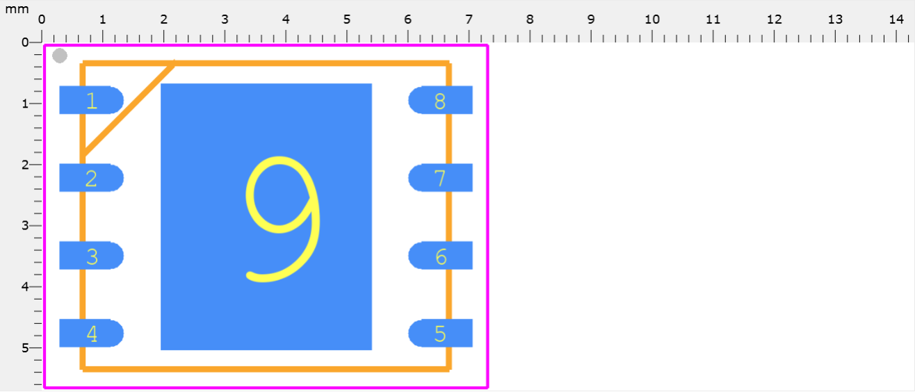
8-WDFN Exposed Pad
供应商器件封装
8-WSON (6x5)
电压 - 电源
2.7 V ~ 3.6 V
内存类型
Non-Volatile
内存大小
128Mb (16M x 8)
访问时间
-
时钟频率
133MHz
内存格式
Flash
写入周期时间 - 字、页
3ms
内存接口
SPI - Quad I/O
请求报价
请填写所有必填字段并点击“提交”,我们将在12小时内通过电子邮件与您联系。如果您有任何问题,请留言或发送电子邮件至 1943626632@qq.com,我们将尽快回复。
有货 28068 PCS
联系信息
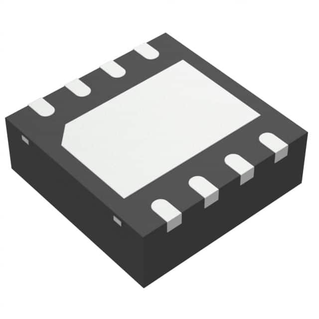
more_pkgimg
more_schimg

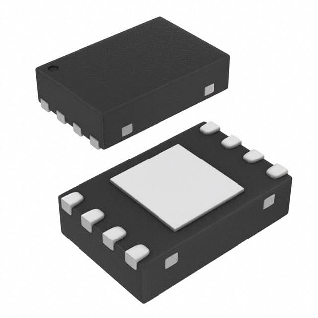
more_3dimg
more_desctext
128M-bit Serial Flash Memory with uniform 4KB sectors and Dual/Quad SPI
Pin Count--------9
Part Category--------Integrated Circuit
Package Category--------Small Outline No-lead
Footprint Name--------Small Outline No-lead - WSON-8 6x5-mm_2022
Pin Count--------9
Part Category--------Integrated Circuit
Package Category--------Small Outline No-lead
Footprint Name--------Small Outline No-lead - WSON-8 6x5-mm_2022
download_pdf
more_faq
W25Q128JVPIQ Frequently Asked Questions (FAQs)
What is the maximum number of erase cycles for the W25Q128JVPIQ?
The W25Q128JVPIQ has a minimum of 100,000 erase cycles per sector, and a maximum of 1,000,000 erase cycles per sector, depending on the operating conditions.
How do I handle the hold signal (HOLD#) during read and write operations?
The HOLD# signal should be kept low during read and write operations. If the HOLD# signal is asserted high, the device will enter a 'hold' state, and all operations will be paused until the HOLD# signal is de-asserted.
What is the purpose of the WP# (Write Protect) pin?
The WP# pin is used to enable or disable the write protection feature. When the WP# pin is tied low, the write protection is enabled, and the device will not allow any write operations. When the WP# pin is tied high, the write protection is disabled, and the device will allow write operations.
How do I determine the device density and organization?
The W25Q128JVPIQ has a density of 128 Mbits, organized as 16,384 x 8,192 bytes. The device is divided into 2,048 sectors, each containing 64 Kbytes.
What is the recommended power-up sequence for the W25Q128JVPIQ?
The recommended power-up sequence is to apply VCC first, followed by VPP (if used), and then the clock signal. The device should be powered up in the following order: VCC, VPP, and then clock.
相关产品

关键词 W25Q128JVPIQ
W25Q128JVPIQ 电子元件
W25Q128JVPIQ 销售
W25Q128JVPIQ 供应商
W25Q128JVPIQ 分销商
W25Q128JVPIQ 数据表
W25Q128JVPIQ 图片
W25Q128JVPIQ 报价
W25Q128JVPIQ 提供
W25Q128JVPIQ 最低价格
W25Q128JVPIQ 搜索
W25Q128JVPIQ 购买
W25Q128JVPIQ 芯片
×
![]()